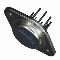
PA08 Cirrus Logic Inc, PA08 Datasheet - Page 4

PA08
Manufacturer Part Number
PA08
Description
OP AMP 300V .15A TO-3-8 CE
Manufacturer
Cirrus Logic Inc
Series
Apex Precision Power™r
Specifications of PA08
Amplifier Type
Power
Number Of Circuits
1
Slew Rate
30 V/µs
Gain Bandwidth Product
5MHz
Current - Input Bias
5pA
Voltage - Input Offset
500µV
Current - Supply
6mA
Current - Output / Channel
150mA
Voltage - Supply, Single/dual (±)
30 V ~ 300 V, ±15 V ~ 150 V
Operating Temperature
-25°C ~ 85°C
Mounting Type
Through Hole
Package / Case
TO-3-8
Number Of Channels
1
Voltage Gain Db
118 dB
Common Mode Rejection Ratio (min)
130 dB
Input Offset Voltage
2 mV
Maximum Operating Temperature
+ 85 C
Mounting Style
Through Hole
Maximum Dual Supply Voltage
+/- 150 V
Minimum Operating Temperature
- 25 C
Lead Free Status / RoHS Status
Lead free / RoHS Compliant
Output Type
-
-3db Bandwidth
-
Lead Free Status / Rohs Status
Details
Other names
598-1296
Available stocks
Company
Part Number
Manufacturer
Quantity
Price
Company:
Part Number:
PA08
Manufacturer:
Cirrus Logic Inc
Quantity:
135
Part Number:
PA08A
Manufacturer:
APEX
Quantity:
20 000
Part Number:
PA08M
Manufacturer:
APEX
Quantity:
20 000
Part Number:
PA08M/883
Manufacturer:
APEX
Quantity:
20 000
PA08 • PA08A
GENERAL
ations" which covers stability, supplies, heat sinking, mounting,
current limit, SOA interpretation, and specification interpretation.
Visit www.Cirrus.com for design tools that help automate tasks
such as calculations for stability, internal power dissipation, cur-
rent limit and heat sink selection. The "Application Notes" and
"Technical Seminar" sections contain a wealth of information
on specific types of applications. Package outlines, heat sinks,
mounting hardware and other accessories are located in the
"Packages and Accessories" section. Evaluation Kits are avail-
able for most Apex Precision Power product models, consult
the "Evaluation Kit" section for details. For the most current
version of all Apex Precision Power product data sheets, visit
www.Cirrus.com.
SAFE OPERATING AREA (SOA)
limitations:
1. The current handling capability of the transistor geometry
2. The second breakdown effect which occurs whenever the
given application, the direction and magnitude of the output
current should be calculated or measured and checked against
the SOA curves. This is simple for resistive loads but more
complex for reactive and EMF generating loads. However, the
following guidelines may save extensive analytical efforts.
1. Under transient conditions, the following capacitive and
2. The amplifier can handle any EMF generating or reactive
4
Please read Application Note 1 "General Operating Consider-
The output stage of most power amplifiers has two distinct
The SOA curves combine the effect of these limits. For a
and the wire bonds.
simultaneous collector current and collector-emitter voltage
exceeds specified limits.
inductive loads are safe with the current limits set to the
maximum:
load and short circuits to the supply rails or simple shorts
to common if the current limits are set as follows:
200
150
100
40
50
30
20
80
150V
125V
100V
80
75V
50V
±V
SUPPLY TO OUTPUT DIFFERENTIAL VOLTAGE (V)
S
100
120
C(MAX)
100µF
10µF
.4µF
.9µF
2µF
150 170
200
1200mH
L(MAX)
280mH
380mH
500mH
250
13H
300
P r o d u c t I n n o v a t i o n F r o m
These simplified limits may be exceeded with further analysis
3. The output stage is protected against transient flyback.
INDUCTIVE LOADS
to protect these amplifiers from flyback (kickback) pulses
exceeding the supply voltages of the amplifier when driving
inductive loads. For component selection, these external diodes
must be very quick, such as ultra fast recovery diodes with no
more than 200 nanoseconds of reverse recovery time. The
diode will turn on to divert the flyback energy into the supply
rails thus protecting the output transistors from destruction due
to reverse bias.
PROTECTION, INDUCTIVE LOAD
pulse must be absorbed by the power supply. As a result, a tran-
sient will be superimposed on the supply voltage, the magnitude
of the transient being a function of its transient impedance and
current sinking capability. If the supply voltage plus transient
exceeds the maximum supply rating or if the AC impedance of
the supply is unknown, it is best to clamp the output and the
supply with a zener diode to absorb the transient.
INPUT PROTECTION
the supply rails and differential voltages up to ±50V. Increased
protection against differential input voltages can be obtained by
adding 2 resistors, 2 capacitors and 4 diode connected FETs
as shown in Figure 2.
CURRENT LIMITING
tors, connected as shown in the external connection diagram.
The minimum value for R
reliability it should be set as high as possible. Refer to the
“General Operating Considerations” section of the handbook
for current limit adjust details.
Fig. 1
Two external diodes as shown in Figure 1, are required
A note of caution about the supply. The energy of the flyback
The input is protected against common mode voltages up to
Proper operation requires the use of two current limit resis-
using the operating conditions for a specific application.
However, for protection against sustained, high energy
flyback, external fast-recovery diodes should be used.
150V
125V
100V
75V
50V
±V
+V
S
S
–V
S
C, L, OR EMF LOAD
SHORT TO ±V
IN4936 OR
UES1106
130mA
20mA
27mA
42mA
67mA
CL
is 3.24Ω. However, for optimum
Fig. 2
+IN
–IN
PROTECTION, OVERVOLTAGE
SC,
Q1
150KΩ
150KΩ
Q2
100pf/200V
100pf/200V
SHORT TO
COMMON
130mA
200mA
200mA
67mA
90mA
Q4
Q3
PA08U
_
+


