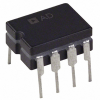
AD708BQ Analog Devices Inc, AD708BQ Datasheet - Page 10

AD708BQ
Manufacturer Part Number
AD708BQ
Description
IC OPAMP GP DUAL PREC 8CDIP
Manufacturer
Analog Devices Inc
Specifications of AD708BQ
Slew Rate
0.3 V/µs
Rohs Status
RoHS non-compliant
Amplifier Type
General Purpose
Number Of Circuits
2
-3db Bandwidth
900kHz
Current - Input Bias
500pA
Voltage - Input Offset
5µV
Current - Supply
4.5mA
Voltage - Supply, Single/dual (±)
6 V ~ 36 V, ±3 V ~ 18 V
Operating Temperature
-40°C ~ 85°C
Mounting Type
Through Hole
Package / Case
8-CDIP (0.300", 7.62mm)
Op Amp Type
Low Offset Voltage
No. Of Amplifiers
2
Bandwidth
900kHz
Supply Voltage Range
± 3V To ± 18V
Amplifier Case Style
DIP
No. Of Pins
8
Channel Separation
140
Common Mode Rejection Ratio
140
Current, Input Bias
0.5 nA
Current, Input Offset
0.1 nA
Current, Offset, Input
0.1 nA (Typ.)
Current, Supply
4.5 mA (Typ.) (Quiescent)
Impedance, Thermal
110 °C/W
Input Resistance
200 Megohms (Typ.)
Number Of Amplifiers
Dual
Package Type
CDIP-8
Power Dissipation
135 mW
Resistance, Input
200 Megohms (Differential), 400 Gigaohms (Common-Mode)
Temperature, Operating, Maximum
85 °C
Temperature, Operating, Minimum
-40 °C
Temperature, Operating, Range
-40 to +85 °C
Voltage, Input
±22 V
Voltage, Noise
10.3 nV/sqrt Hz
Voltage, Offset
5 μV
Voltage, Offset, Input
5 μV (Typ.)
Voltage, Output, High
+14 V
Voltage, Output, Low
-14 V
Voltage, Supply
±15 V
Output Type
-
Current - Output / Channel
-
Gain Bandwidth Product
-
Lead Free Status / RoHS Status
Contains lead / RoHS non-compliant
Available stocks
Company
Part Number
Manufacturer
Quantity
Price
Company:
Part Number:
AD708BQ
Manufacturer:
SEMTECH
Quantity:
1 000
AD708
THEORY OF OPERATION
CROSSTALK PERFORMANCE
The AD708 exhibits very low crosstalk as shown in Figure 25,
Figure 26, and Figure 27. Figure 25 shows the offset voltage
induced on Side B of the AD708 when Side A output is moving
slowly (0.2 Hz) from −10 V to +10 V under no load. This is the
least stressful situation to the part because the overall power in
the chip does not change. Only the location of the power in the
output device changes. Figure 26 shows the input offset voltage
change to Side B when Side A is driving a 2 kΩ load. Here the
power changes in the chip with the maximum power change
occurring at 7.5 V. Figure 27 shows crosstalk under the most
severe conditions. Side A is connected as a follower with
0 V input, and is forced to sink and source ±5 mA of output
current.
Even this large change in power causes only an 8 μV (linear)
change in the input offset voltage of Side B.
Power = (30 V)(5 mA) = 150 mW
V
10Ω
Figure 25. Crosstalk with No Load
IN
= ±10V
10Ω
V
OUTA
= 2V/DIV
A
10kΩ
B
V
V
OUTA
OUTB
2V
Rev. C | Page 10 of 16
Figure 27. Crosstalk Under Forced Source and Sink Conditions
Figure 26. Crosstalk with 2 kΩ Load
V
10Ω
10Ω
IN
= ±10V
10Ω
10Ω
V
IN
OUTA
A
= 1mA/DIV
= 2V/DIV
A
B
A
B
10kΩ
10kΩ
I
IN
2kΩ
2kΩ
= ±5mA
V
V
OUTA
OUTB
V
V
2V
2V
OUTB
IN
= ±10V


