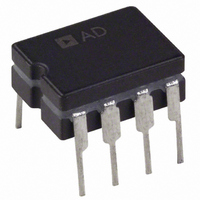
AD712AQ Analog Devices Inc, AD712AQ Datasheet - Page 12

AD712AQ
Manufacturer Part Number
AD712AQ
Description
IC OPAMP BIFET DUAL PREC 8CDIP
Manufacturer
Analog Devices Inc
Specifications of AD712AQ
Slew Rate
20 V/µs
Rohs Status
RoHS non-compliant
Amplifier Type
J-FET
Number Of Circuits
2
-3db Bandwidth
4MHz
Current - Input Bias
25pA
Voltage - Input Offset
300µV
Current - Supply
5mA
Current - Output / Channel
25mA
Voltage - Supply, Single/dual (±)
9 V ~ 36 V, ±4.5 V ~ 20 V
Operating Temperature
-40°C ~ 85°C
Mounting Type
Through Hole
Package / Case
8-CDIP (0.300", 7.62mm)
Op Amp Type
Precision
No. Of Amplifiers
2
Bandwidth
4MHz
Supply Voltage Range
± 4.5V To ± 18V
Amplifier Case Style
DIP
No. Of Pins
8
Operating Temperature Range
-40°C To +85°C
Common Mode Rejection Ratio
88
Current, Input Bias
25 pA
Current, Input Offset
10 pA
Current, Offset, Input
10 pA (Typ.)
Current, Output
±25 mA
Current, Supply
5 mA (Typ.)
Harmonic Distortion
0.0003 %
Impedance, Thermal
22 °C/W
Number Of Amplifiers
Dual
Package Type
CDIP-8
Resistance, Input
3×10^12 Ohms
Temperature, Operating, Maximum
85 °C
Temperature, Operating, Minimum
-40 °C
Temperature, Operating, Range
-40 to +85 °C
Voltage, Input
±20 V (Differential), -11.5 to +14.5 V (Common-Mode)
Voltage, Noise
45 nV/sqrt Hz
Voltage, Offset
0.3 mV
Voltage, Offset, Input
0.3 mV (Typ.)
Voltage, Output, High
+13.9 V
Voltage, Output, Low
-13.3 V
Voltage, Supply
±15 V
Output Type
-
Gain Bandwidth Product
-
Lead Free Status / RoHS Status
Contains lead / RoHS non-compliant
Available stocks
Company
Part Number
Manufacturer
Quantity
Price
Company:
Part Number:
AD712AQ
Manufacturer:
SKYWORKS
Quantity:
15 600
Part Number:
AD712AQ
Manufacturer:
ADI/亚德诺
Quantity:
20 000
Company:
Part Number:
AD712AQ/CQ
Manufacturer:
AD
Quantity:
5 510
Company:
Part Number:
AD712AQ/CQ
Manufacturer:
AGILENT
Quantity:
5 510
AD712
OP AMP SETTLING TIME—A MATHEMATICAL
MODEL
The design of the AD712 gives careful attention to optimizing
individual circuit components; in addition, a careful trade-off
was made: the gain bandwidth product (4 MHz) and slew rate
(20 V/μs) were chosen to be high enough to provide very fast
settling time but not too high to cause a significant reduction
in phase margin (and therefore, stability). Thus designed, the
AD712 settles to ±0.01%, with a 10 V output step, in under 1 μs,
while retaining the ability to drive a 250 pF load capacitance
when operating as a unity-gain follower.
If an op amp is modeled as an ideal integrator with a unity-gain
crossover frequency of ω
describes the small signal behavior of the circuit of Figure 32,
consisting of an op amp connected as an I-to-V converter at the
output of a bipolar or CMOS DAC. This equation would com-
pletely describe the output of the system if not for the finite slew
rate and other nonlinear effects of the op amp.
Where
G
This equation can then be solved for C
In these equations, Capacitance C
appearing at the inverting terminal of the op amp. When
modeling a DAC buffer application, the Norton equivalent
circuit shown in Figure 32 can be used directly; Capacitance C
is the total capacitance of the output of the DAC plus the input
capacitance of the op amp (because the two are in parallel).
ω
2
Figure 32. Simplified Model of the AD712 Used as a Current-Out DAC Buffer
N
π
O
= noise gain of circuit
= unity-gain frequency of the op amp.
C
V
I
IN
X
O
I
=
O
=
2
R
−
R
ω
G
R
(
ω
O
C
O
N
O
X
+
)
s
2
2
C
RC
+
X
⎛
⎜
⎜
⎝
X
G
ω
ω
O
−
AD712
+
–
/2π, then Equation 1 accurately
O
R
N
O
⎛
⎜ ⎜
⎝
R
1
1/2
+
ω
+
+
O
(
1
RC
R
−
R
O
G
C
f
X
R
F
⎞
⎟ ⎟
⎠
N
⎞
⎟
⎟
⎠
is the total capacitance
)
.
s
+
f
1
R
L
C
L
V
OUT
Rev. H | Page 12 of 20
(1)
(2)
X
When R
equivalents, the general-purpose inverting amplifier shown in
Figure 33 is created. Note that when using this general model,
Capacitance C
a simple inverting op amp is being simulated, or the combined
capacitance of the DAC output and the op amp input if the
DAC buffer is being modeled.
In either case, Capacitance C
one-pole to a two-pole response; this additional pole increases
settling time by introducing peaking or ringing in the op amp
output. Because the value of C
accuracy, Equation 2 can be used to choose a small capacitor
(C
Figure 34 is a graphical solution of Equation 2 for the AD712
with R = 4 kΩ.
F
) to cancel the input pole and optimize amplifier response.
V
60
50
40
30
20
10
Figure 33. Simplified Model of the AD712 Used as an Inverter
IN
0
O
0
and I
Figure 34. Value of Capacitor C
R
IN
X
O
G
is either the input capacitance of the op amp, if
10
are replaced with their Thevenin V
N
= 4.0
G
N
C
X
= 3.0
20
+
AD712
–
1/2
X
X
causes the system to go from a
can be estimated with reasonable
C
30
C
F
R
F
F
vs. Value of C
40
R
L
G
G
G
N
N
N
= 1.5
= 2.0
= 1.0
C
L
50
X
V
IN
OUT
and R
60
IN


