ADM4073FWRJZ-REEL7 Analog Devices Inc, ADM4073FWRJZ-REEL7 Datasheet
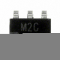
IC AMP CS 1.8MHZ SOT23-6

ADM4073FWRJZ-REEL7

Manufacturer Part Number
ADM4073FWRJZ-REEL7
Description
IC AMP CS 1.8MHZ SOT23-6
Manufacturer
Analog Devices Inc
Datasheet

Specifications of ADM4073FWRJZ-REEL7

Amplifier Type
Current Sense
Number Of Circuits
1
Gain Bandwidth Product
1.8MHz
Current - Input Bias
40µA
Voltage - Input Offset
1000µV
Current - Supply
500µA
Voltage - Supply, Single/dual (±)
3 V ~ 28 V
Operating Temperature
-40°C ~ 125°C
Mounting Type
Surface Mount
Package / Case
SOT-23-6
No. Of Amplifiers
1
Input Bias Current
120µA
Input Offset Voltage
1mV
Bandwidth
1.7MHz
Cmrr
90dB
Supply Voltage Range
3V To 28V
Supply Current
500µA
Amplifier Case Style
SOT-23
Rohs Compliant
Yes
Lead Free Status / RoHS Status
Lead free / RoHS Compliant
Output Type
-
Current - Output / Channel
-
-3db Bandwidth
-
Slew Rate
-
Other names
ADM4073FWRJZ-REEL7TR

Available stocks

Company
Part Number
Manufacturer
Quantity
Price
Part Number:
ADM4073FWRJZ-REEL7
Manufacturer:
TI
Quantity:
460
Part Number:
ADM4073FWRJZ-REEL7
Manufacturer:
ADI/亚德诺
Quantity:
20 000
FEATURES
Low cost, compact, current-sense solution
3 available gain versions
Typical ±1.0% full-scale accuracy
Supply current: 500 μA
Wide bandwidth: 1.8 MHz
Operating supply: 3 V to 28 V
Wide common-mode range: 2 V to 28 V
Operating temperature range: −40°C to +125°C
Available in a 6-lead SOT-23 package
Pin-to-pin compatibility with the MAX4073
APPLICATIONS
Cell phones
PDAs
Notebook computers
Portable, battery-powered systems
Smart battery packs and chargers
Automotive
Power management systems
PA bias control
General system-level, board-level current monitoring
Precision current sources
GENERAL DESCRIPTION
The ADM4073 is a low cost, high-side, current-sense amplifier
ideal for small portable applications, such as cell phones,
notebook computers, PDAs, and other systems where current
monitoring is required. The device is available in three different
gain models, eliminating the need for gain-setting resistors.
Because the ground path is not interrupted, the ADM4073 is
particularly useful in rechargeable battery-powered systems,
while its wide 1.8 MHz bandwidth makes it suitable for use
inside battery-charger control loops. The input common-mode
range of 2 V to 28 V is independent of the supply voltage.
Rev. A
Information furnished by Analog Devices is believed to be accurate and reliable. However, no
responsibility is assumed by Analog Devices for its use, nor for any infringements of patents or other
rights of third parties that may result from its use. Specifications subject to change without notice. No
license is granted by implication or otherwise under any patent or patent rights of Analog Devices.
Trademarks and registered trademarks are the property of their respective owners.
Independent of supply voltage
20 V/V (ADM4073T)
50 V/V (ADM4073F)
100 V/V (ADM4073H)
High-Side, Current-Sense Amplifier
One Technology Way, P.O. Box 9106, Norwood, MA 02062-9106, U.S.A.
Tel: 781.329.4700
Fax: 781.461.3113
The voltage on the output pin is determined by the current
flowing through the selectable external sense resistor and the
gain of the version selected. The operating range is 3 V to 28 V
with a typical supply current of 500 μA.
The ADM4073 is available in a 6-lead SOT-23 package and is
specified over the automotive operating temperature range
(−40°C to +125°C).
3V TO 28V
2V TO 28V
2V TO 28V
3V TO 28V
0.1µF
Low Cost, Voltage Output,
FUNCTIONAL BLOCK DIAGRAM
0.1µF
APPLICATION DIAGRAM
V
©2006–2008 Analog Devices, Inc. All rights reserved.
CC
CURRENT
V
MIRROR
RG1
CC
RS+
RS+
GND
ADM4073
I
R
RGD
ADM4073
GND
Figure 1.
SENSE
Figure 2.
R
I
SENSE
RG1
AV
RS–
OUT
I
RGD = 12kΩ
LOAD
RS–
RG2
ADM4073
OUT
ADC
www.analog.com
V
V
OUT
OUT
V
OUT

Related parts for ADM4073FWRJZ-REEL7

ADM4073FWRJZ-REEL7 Summary of contents

Page 1

FEATURES Low cost, compact, current-sense solution 3 available gain versions 20 V/V (ADM4073T) 50 V/V (ADM4073F) 100 V/V (ADM4073H) Typical ±1.0% full-scale accuracy Supply current: 500 μA Wide bandwidth: 1.8 MHz Operating supply Wide common-mode ...

Page 2

ADM4073 TABLE OF CONTENTS Features .............................................................................................. 1 Applications ....................................................................................... 1 Functional Block Diagram .............................................................. 1 Application Diagram ........................................................................ 1 General Description ......................................................................... 1 Revision History ............................................................................... 2 Specifications ..................................................................................... 3 Absolute Maximum Ratings ............................................................ 4 Thermal Characteristics .............................................................. 4 REVISION ...

Page 3

SPECIFICATIONS − RS+ SENSE RS+ RS− Table 1. Parameter POWER SUPPLY Operating Voltage Range Common-Mode Input Range, V CMR Common-Mode Input Rejection, ...

Page 4

ADM4073 ABSOLUTE MAXIMUM RATINGS Table 2. Parameter V to GND CC RS+, RS− to GND OUT to GND OUT Short-Circuit to GND Differential Input Voltage (V − RS+ RS− Current into Any Pin Storage Temperature Range Operating Temperature ...

Page 5

PIN CONFIGURATION AND FUNCTION DESCRIPTIONS Table 4. Pin Function Descriptions Pin No. Mnemonic Description 1 GND Chip Ground Pin. 2 GND Chip Ground Pin Chip Power Supply. Requires a 0.1 μF capacitor to ground RS+ Power-Side ...

Page 6

ADM4073 TYPICAL PERFORMANCE CHARACTERISTICS 0. 6.25mV SENSE 0.55 0.50 ADM4073H 0.45 0.40 ADM4073T 0.35 0. SUPPLY VOLTAGE (V) Figure 4. Supply Current vs. Supply Voltage (V 1 100mV SENSE 1.4 1.3 1.2 ...

Page 7

V = 6.25mV SENSE 0.8 0.6 0.4 ADM4073F 0.2 0 ADM4073T –0.2 –0.4 –0.6 ADM4073H –0.8 –1 SUPPLY VOLTAGE (V) Figure 10. Total Output Error vs. Supply Voltage (V 1.0 ADM4073F 0.5 ADM4073H 0 ...

Page 8

ADM4073 45 ADM4073H 40 ADM4073F 35 30 ADM4073T 0 100 FREQUENCY (kHz) Figure 16. Small Signal Gain vs. Frequency V SENSE 2.5mV/DIV OUT 50mV/DIV 1µs/DIV Figure 17. ADM4073T Small Signal Transient Response ...

Page 9

V SENSE 45mV/DIV OUT 4.7V/DIV 1µs/DIV Figure 22. ADM4073H Large Signal Transient Response SENSE 100mV/DIV OUT 600mV/DIV 1µs/DIV Figure 23. ADM4073T Overdrive Response 100mV V CC 6.25mV 2V/DIV 10V ...

Page 10

ADM4073 THEORY OF OPERATION The current from the source flows through R erates a voltage drop across the RS+ and RS− terminals SENSE of the sense amplifier. The Input Stage Amplifier A1 regulates its inputs to be equal, ...

Page 11

... OUTLINE DIMENSIONS INDICATOR 0.15 MAX ORDERING GUIDE Model Gain 1 ADM4073TWRJZ-REEL7 20 1 ADM4073FWRJZ-REEL7 50 1 ADM4073HWRJZ-REEL7 100 1, 2 ADM4073WFWRJZ-RL7 RoHS Compliant Part. 2 Automotive Grade. 2.90 BSC 2.80 BSC 1.60 BSC PIN 1 0.95 BSC 1.90 1.30 BSC 1.15 0.90 1.45 MAX 0.22 0.08 0.50 SEATING 0 ...

Page 12

ADM4073 NOTES ©2006–2008 Analog Devices, Inc. All rights reserved. Trademarks and registered trademarks are the property of their respective owners. D05131-0-10/08(A) Rev Page ...

Related keywords