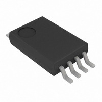
MCP6022-E/ST Microchip Technology, MCP6022-E/ST Datasheet - Page 17

MCP6022-E/ST
Manufacturer Part Number
MCP6022-E/ST
Description
IC OPAMP DUAL 2.5V 10MHZ 8-TSSOP
Manufacturer
Microchip Technology
Datasheet
1.MCP6021-ESN.pdf
(42 pages)
Specifications of MCP6022-E/ST
Slew Rate
7 V/µs
Amplifier Type
General Purpose
Number Of Circuits
2
Output Type
Rail-to-Rail
Gain Bandwidth Product
10MHz
Current - Input Bias
1pA
Voltage - Input Offset
500µV
Current - Supply
1mA
Current - Output / Channel
30mA
Voltage - Supply, Single/dual (±)
2.5 V ~ 5.5 V
Operating Temperature
-40°C ~ 125°C
Mounting Type
Surface Mount
Package / Case
8-TSSOP
Op Amp Type
Rail To Rail
No. Of Amplifiers
2
Bandwidth
10MHz
Supply Voltage Range
2.5V To 5.5V
Amplifier Case Style
TSSOP
No. Of Pins
8
Number Of Channels
2
Voltage Gain Db
110 dB
Common Mode Rejection Ratio (min)
70 dB
Input Offset Voltage
0.25 mV
Operating Supply Voltage
3 V, 5 V
Supply Current
2.7 mA
Maximum Operating Temperature
+ 125 C
Mounting Style
SMD/SMT
Minimum Operating Temperature
- 40 C
Lead Free Status / RoHS Status
Lead free / RoHS Compliant
-3db Bandwidth
-
Lead Free Status / Rohs Status
Details
4.0
The MCP6021/1R/2/3/4 family of operational amplifiers
are fabricated on Microchip’s state-of-the-art CMOS
process. They are unity-gain stable and suitable for a
wide range of general-purpose applications.
4.1
4.1.1
The MCP6021/1R/2/3/4 op amp is designed to prevent
phase reversal when the input pins exceed the supply
voltages.
ing the supply voltage without any phase reversal.
4.1.2
The ESD protection on the inputs can be depicted as
shown in
protect the input transistors, and to minimize input bias
current (I
when they try to go more than one diode drop below
V
above V
allow normal operation, and low enough to bypass
quick ESD events within the specified limits.
FIGURE 4-1:
Structures.
In order to prevent damage and/or improper operation
of these op amps, the circuit they are in must limit the
currents and voltages at the V
Absolute Maximum Ratings † at the beginning of
Section 1.0 “Electrical Characteristics”).
shows the recommended approach to protecting these
inputs. The internal ESD diodes prevent the input pins
(V
the resistors R
out of the input pins. Diodes D
input pins (V
V
implemented as shown, resistors R
the current through D
© 2009 Microchip Technology Inc.
SS
DD
IN
. They also clamp any voltages that go too far
+ and V
, and dump any currents onto V
V
V
V
IN
DD
SS
+
DD
APPLICATIONS INFORMATION
Rail-to-Rail Input
B
Figure 2-42
). The input ESD diodes clamp the inputs
Figure
; their breakdown voltage is high enough to
Bond
Bond
Bond
PHASE REVERSAL
LIMITS
Pad
Pad
Pad
IN
IN
–) from going too far below ground, and
INPUT VOLTAGE AND CURRENT
1
+ and V
and R
4-1. This structure was chosen to
1
shows the input voltage exceed-
2
Simplified Analog Input ESD
and D
limit the possible current drawn
IN
Stage
Input
–) from going too far above
2
.
IN
1
+ and V
and D
1
and R
Bond
Pad
2
IN
prevent the
– pins (see
DD
2
Figure 4-2
V
also limit
. When
IN
–
FIGURE 4-2:
Inputs.
It is also possible to connect the diodes to the left of
resistors R
diodes D
mechanism. The resistors then serve as in-rush current
limiters; the DC current into the input pins (V
V
A significant amount of current can flow out of the
inputs when the common mode voltage (V
ground (V
high impedance may need to limit the useable voltage
range.
4.1.3
The input stage of the MCP6021/1R/2/3/4 op amps use
two differential CMOS input stages in parallel. One
operates at low common mode input voltage (V
while the other operates at high V
ogy, the device operates with Vcm up to 0.3V above
V
4.2
The Maximum Output Voltage Swing is the maximum
swing possible under a particular output load.
According to the specification table, the output can
reach within 20 mV of either supply rail when
R
information concerning typical performance.
4.3
Driving large capacitive loads can cause stability
problems for voltage feedback op amps. As the load
capacitance increases, the feedback loop’s phase
margin decreases, and the closed loop bandwidth is
reduced. This produces gain-peaking in the frequency
response, with overshoot and ringing in the step
response.
IN
DD
L
–) should be very small.
= 10 kΩ. See
and 0.3V below V
V
V
MCP6021/1R/2/3/4
1
2
1
Rail-to-Rail Output
Capacitive Loads
SS
1
and D
NORMAL OPERATION
); see
R
R
and R
R
R
1
2
D
1
2
>
>
Figure 2-31
2
1
V
V
2
needs to be limited by some other
SS
SS
Figure
. In this case, current through the
D
SS
Protecting the Analog
– (minimum expected V
– (minimum expected V
2
.
2-42. Applications that are
and
MCP602X
2 mA
2 mA
V
Figure 2-34
R
CM
DD
3
DS21685D-page 17
. WIth this topol-
CM
) is below
for more
1
2
IN
)
)
+ and
CM
),


