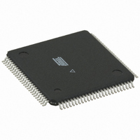
ATMEGA6450-16AI Atmel, ATMEGA6450-16AI Datasheet - Page 192

ATMEGA6450-16AI
Manufacturer Part Number
ATMEGA6450-16AI
Description
IC AVR MCU FLASH 64K 5V 100TQFP
Manufacturer
Atmel
Series
AVR® ATmegar
Datasheet
1.ATMEGA325-16MU.pdf
(362 pages)
Specifications of ATMEGA6450-16AI
Core Processor
AVR
Core Size
8-Bit
Speed
16MHz
Connectivity
SPI, UART/USART, USI
Peripherals
Brown-out Detect/Reset, POR, PWM, WDT
Number Of I /o
68
Program Memory Size
64KB (32K x 16)
Program Memory Type
FLASH
Eeprom Size
2K x 8
Ram Size
4K x 8
Voltage - Supply (vcc/vdd)
2.7 V ~ 5.5 V
Data Converters
A/D 8x10b
Oscillator Type
Internal
Operating Temperature
-40°C ~ 85°C
Package / Case
100-TQFP, 100-VQFP
For Use With
ATSTK600-TQFP100 - STK600 SOCKET/ADAPTER 100-TQFPATSTK504 - STARTER KIT AVR EXP MOD 100P LCD
Lead Free Status / RoHS Status
Contains lead / RoHS non-compliant
Available stocks
Company
Part Number
Manufacturer
Quantity
Price
- Current page: 192 of 362
- Download datasheet (7Mb)
20.3
20.3.1
20.3.2
20.3.3
20.3.4
20.3.5
20.4
20.4.1
2570M–AVR–04/11
Alternative USI Usage
Register Descriptions
Half-duplex Asynchronous Data Transfer
4-bit Counter
12-bit Timer/Counter
Edge Triggered External Interrupt
Software Interrupt
USIDR – USI Data Register
trol Unit will hold the SCL low until the slave is ready to receive more data. This may reduce the
actual data rate in two-wire mode.
When the USI unit is not used for serial communication, it can be set up to do alternative tasks
due to its flexible design.
By utilizing the Shift Register in Three-wire mode, it is possible to implement a more compact
and higher performance UART than by software only.
The 4-bit counter can be used as a stand-alone counter with overflow interrupt. Note that if the
counter is clocked externally, both clock edges will generate an increment.
Combining the USI 4-bit counter and Timer/Counter0 allows them to be used as a 12-bit
counter.
By setting the counter to maximum value (F) it can function as an additional external interrupt.
The Overflow Flag and Interrupt Enable bit are then used for the external interrupt. This feature
is selected by the USICS1 bit.
The counter overflow interrupt can be used as a software interrupt triggered by a clock strobe.
The USI uses no buffering of the Serial Register, i.e., when accessing the Data Register
(USIDR) the Serial Register is accessed directly. If a serial clock occurs at the same cycle the
register is written, the register will contain the value written and no shift is performed. A (left) shift
operation is performed depending of the USICS1..0 bits setting. The shift operation can be con-
trolled by an external clock edge, by a Timer/Counter0 Compare Match, or directly by software
using the USICLK strobe bit. Note that even when no wire mode is selected (USIWM1..0 = 0)
both the external data input (DI/SDA) and the external clock input (USCK/SCL) can still be used
by the Shift Register.
The output pin in use, DO or SDA depending on the wire mode, is connected via the output latch
to the most significant bit (bit 7) of the Data Register. The output latch is open (transparent) dur-
ing the first half of a serial clock cycle when an external clock source is selected (USICS1 = 1),
and constantly open when an internal clock source is used (USICS1 = 0). The output will be
changed immediately when a new MSB written as long as the latch is open. The latch ensures
that data input is sampled and data output is changed on opposite clock edges.
Bit
(0xBA)
Read/Write
Initial Value
MSB
R/W
7
0
R/W
6
0
R/W
5
0
R/W
4
0
ATmega325/3250/645/6450
R/W
3
0
R/W
2
0
R/W
1
0
LSB
R/W
0
0
USIDR
192
Related parts for ATMEGA6450-16AI
Image
Part Number
Description
Manufacturer
Datasheet
Request
R

Part Number:
Description:
Manufacturer:
Atmel Corporation
Datasheet:

Part Number:
Description:
IC AVR MCU FLASH 64K 64TQFP
Manufacturer:
Atmel
Datasheet:

Part Number:
Description:
IC AVR MCU FLASH 64K 5V 64TQFP
Manufacturer:
Atmel
Datasheet:

Part Number:
Description:
IC AVR MCU FLASH 64K 64-QFN
Manufacturer:
Atmel
Datasheet:

Part Number:
Description:
MCU AVR 64KB FLASH 16MHZ 64TQFP
Manufacturer:
Atmel
Datasheet:

Part Number:
Description:
MCU AVR 64KB FLASH 16MHZ 64QFN
Manufacturer:
Atmel
Datasheet:

Part Number:
Description:
IC AVR MCU FLASH 64K 5V 64QFN
Manufacturer:
Atmel
Datasheet:

Part Number:
Description:
Manufacturer:
Atmel Corporation
Datasheet:

Part Number:
Description:
Manufacturer:
ATMEL Corporation
Datasheet:

Part Number:
Description:
Manufacturer:
ATMEL Corporation
Datasheet:

Part Number:
Description:
IC AVR MCU 64K 16MHZ 5V 64TQFP
Manufacturer:
Atmel
Datasheet:

Part Number:
Description:
IC AVR MCU 64K 16MHZ 5V 64-QFN
Manufacturer:
Atmel
Datasheet:

Part Number:
Description:
IC AVR MCU 64K 16MHZ COM 64-TQFP
Manufacturer:
Atmel
Datasheet:

Part Number:
Description:
IC AVR MCU 64K 16MHZ IND 64-TQFP
Manufacturer:
Atmel
Datasheet:


