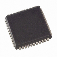
AT89LS8252-12JC Atmel, AT89LS8252-12JC Datasheet - Page 2

AT89LS8252-12JC
Manufacturer Part Number
AT89LS8252-12JC
Description
IC MICRO CTRL 12MHZ 44PLCC
Manufacturer
Atmel
Series
89LSr
Datasheet
1.AT89LS8252-12AC.pdf
(35 pages)
Specifications of AT89LS8252-12JC
Core Processor
8051
Core Size
8-Bit
Speed
12MHz
Connectivity
SPI, UART/USART
Peripherals
POR, WDT
Number Of I /o
32
Program Memory Size
8KB (8K x 8)
Program Memory Type
FLASH
Eeprom Size
2K x 8
Ram Size
256 x 8
Voltage - Supply (vcc/vdd)
2.7 V ~ 6 V
Oscillator Type
Internal
Operating Temperature
0°C ~ 70°C
Package / Case
44-PLCC
Lead Free Status / RoHS Status
Contains lead / RoHS non-compliant
Data Converters
-
Other names
AT89LS825212JC
Available stocks
Company
Part Number
Manufacturer
Quantity
Price
Pin Configurations
Pin Description
V
Supply voltage.
GND
Ground.
Port 0
Port 0 is an 8-bit open drain bidirectional I/O port. As an
output port, each pin can sink eight TTL inputs. When 1s
are written to port 0 pins, the pins can be used as high-
impedance inputs.
Port 0 can also be configured to be the multiplexed low-
order address/data bus during accesses to external pro-
gram and data memory. In this mode, P0 has internal pul-
lups.
2
CC
(MOSI) P1.5
(MISO) P1.6
(RXD) P3.0
(INT0) P3.2
(INT1) P3.3
(SCK) P1.7
(TXD) P3.1
(T0) P3.4
(T1) P3.5
RST
NC
AT89LS8252
(T2 EX) P1.1
(MOSI) P1.5
(MISO) P1.6
(INT0) P3.2
(INT1) P3.3
(SCK) P1.7
(RXD) P3.0
(TXD) P3.1
(WR) P3.6
1
2
3
4
5
6
7
8
9
10
11
(RD) P3.7
(SS) P1.4
(T2) P1.0
(T0) P3.4
(T1) P3.5
XTAL2
XTAL1
GND
P1.2
P1.3
RST
1
2
3
4
5
6
7
8
9
10
11
12
13
14
15
16
17
18
19
20
PDIP
TQFP
40
39
38
37
36
35
34
33
32
31
30
29
28
27
26
25
24
23
22
21
VCC
P0.0 (AD0)
P0.1 (AD1)
P0.2 (AD2)
P0.3 (AD3)
P0.4 (AD4)
P0.5 (AD5)
P0.6 (AD6)
P0.7 (AD7)
EA/VPP
ALE/PROG
PSEN
P2.7 (A15)
P2.6 (A14)
P2.5 (A13)
P2.4 (A12)
P2.3 (A11)
P2.2 (A10)
P2.1 (A9)
P2.0 (A8)
33
32
31
30
29
28
27
26
25
24
23
P0.4 (AD4)
P0.5 (AD5)
P0.6 (AD6)
P0.7 (AD7)
EA/VPP
NC
ALE/PROG
PSEN
P2.7 (A15)
P2.6 (A14)
P2.5 (A13)
Port 0 also receives the code bytes during Flash program-
ming and outputs the code bytes during program verifica-
tion. External pullups are required during program verifica-
tion.
Port 1
Port 1 is an 8-bit bidirectional I/O port with internal pullups.
The Port 1 output buffers can sink/source four TTL inputs.
When 1s are written to Port 1 pins, they are pulled high by
the internal pullups and can be used as inputs. As inputs,
Port 1 pins that are externally being pulled low will source
current (I
Some Port 1 pins provide additional functions. P1.0 and
P1.1 can be configured to be the timer/counter 2 external
count input (P1.0/T2) and the timer/counter 2 trigger input
(P1.1/T2EX), respectively.
IL
) because of the internal pullups.
(MOSI) P1.5
(MISO) P1.6
(INT0) P3.2
(INT1) P3.3
(SCK) P1.7
(RXD) P3.0
(TXD) P3.1
(T0) P3.4
(T1) P3.5
RST
NC
7
8
9
10
11
12
13
14
15
16
17
PLCC
39
38
37
36
35
34
33
32
31
30
29
P0.4 (AD4)
P0.5 (AD5)
P0.6 (AD6)
P0.7 (AD7)
EA/VPP
NC
ALE/PROG
PSEN
P2.7 (A15)
P2.6 (A14)
P2.5 (A13)
0850C–MICRO–3/06


