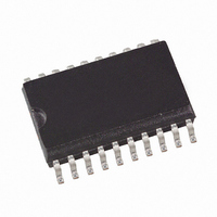
AT90S1200-4YI Atmel, AT90S1200-4YI Datasheet - Page 34

AT90S1200-4YI
Manufacturer Part Number
AT90S1200-4YI
Description
IC MCU 1K FLSH 4MHZ LV IT 20SSOP
Manufacturer
Atmel
Series
AVR® 90Sr
Datasheet
1.AT90S1200-12PC.pdf
(71 pages)
Specifications of AT90S1200-4YI
Core Processor
AVR
Core Size
8-Bit
Speed
4MHz
Connectivity
SPI
Peripherals
POR, WDT
Number Of I /o
15
Program Memory Size
1KB (512 x 16)
Program Memory Type
FLASH
Eeprom Size
64 x 8
Voltage - Supply (vcc/vdd)
2.7 V ~ 6 V
Oscillator Type
Internal
Operating Temperature
-40°C ~ 85°C
Package / Case
20-SSOP
Lead Free Status / RoHS Status
Contains lead / RoHS non-compliant
Ram Size
-
Data Converters
-
Available stocks
Company
Part Number
Manufacturer
Quantity
Price
Part Number:
AT90S1200-4YI
Manufacturer:
ATMEL/爱特梅尔
Quantity:
20 000
Port D
Port D Data Register – PORTD
Port D Data Direction Register
– DDRD
Port D Input Pins Address –
PIND
Port D as General Digital I/O
34
AT90S1200
Three I/O memory address locations are allocated for Port D, one each for the Data
Register – PORTD ($12), Data Direction Register – DDRD ($11), and the Port D Input
Pins – PIND ($10). The Port D Input Pins address is read-only, while the Data Register
and the Data Direction Register are read/write.
Port D has seven bi-directional I/O pins with internal pull-up resistors, PD6..PD0. The
Port D output buffers can sink 20 mA. As inputs, Port D pins that are externally pulled
low will source current if the pull-up resistors are activated.
Some Port D pins have alternate functions as shown in Table 10.
Table 10. Port D Pin Alternate Functions
The Port D Input Pins address (PIND) is not a register, and this address enables access
to the physical value on each Port D pin. When reading PORTD, the Port D Data Latch
is read; and when reading PIND, the logical values present on the pins are read.
PDn, general I/O pin: The DDDn bit in the DDRD Register selects the direction of this
pin. If DDDn is set (one), PDn is configured as an output pin. If DDDn is cleared (zero),
PDn is configured as an input pin. If PORTDn is set (one) when DDDn is configured as
an input pin, the MOS pull-up resistor is activated. To switch the pull-up resistor off, the
PORTDn bit has to be cleared (zero) or the pin has to be configured as an output pin.
The Port D pins are tri-stated when a reset condition becomes active, even if the clock is
not active.
Bit
$12
Read/Write
Initial Value
Bit
$11
Read/Write
Initial Value
Bit
$10
Read/Write
Initial Value
Port Pin
PD2
PD4
R
R
R
7
–
0
7
–
0
7
–
0
PORTD6
PIND6
DDD6
Alternate Function
INT0 (External Interrupt 0 input)
T0 (Timer/Counter 0 external input)
R/W
R/W
N/A
R
6
0
6
6
0
PORTD5
PIND5
DDD5
R/W
R/W
N/A
R
5
0
5
5
0
PORTD4
PIND4
DDD4
R/W
R/W
N/A
R
4
0
4
4
0
PORTD3
PIND3
DDD3
R/W
R/W
N/A
R
3
0
3
3
0
PORTD2
PIND2
DDD2
R/W
N/A
R/W
R
2
0
2
2
0
PORTD1
PIND1
DDD1
R/W
N/A
R/W
R
1
0
1
1
0
PORTD0
PIND0
DDD0
R/W
N/A
R/W
0838H–AVR–03/02
R
0
0
0
0
0
PORTD
DDRD
PIND


