DS80C320-MCG Maxim Integrated Products, DS80C320-MCG Datasheet - Page 5
DS80C320-MCG
Manufacturer Part Number
DS80C320-MCG
Description
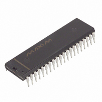
IC MCU HI SPEED 25MHZ 40-DIP
Manufacturer
Maxim Integrated Products
Series
80Cr
Datasheet
1.DS80C323-QND.pdf
(38 pages)
Specifications of DS80C320-MCG
Core Processor
8051
Core Size
8-Bit
Speed
25MHz
Connectivity
EBI/EMI, SIO, UART/USART
Peripherals
Power-Fail Reset, WDT
Number Of I /o
32
Program Memory Type
ROMless
Ram Size
256 x 8
Voltage - Supply (vcc/vdd)
4.5 V ~ 5.5 V
Oscillator Type
External
Operating Temperature
0°C ~ 70°C
Package / Case
40-DIP (0.600", 15.24mm)
Processor Series
DS80C320
Core
8051
Data Bus Width
8 bit
Program Memory Size
64 KB
Data Ram Size
64 KB
Interface Type
UART
Maximum Clock Frequency
25 MHz
Number Of Programmable I/os
32
Number Of Timers
3
Operating Supply Voltage
4.25 V to 5.5 V
Maximum Operating Temperature
+ 70 C
Mounting Style
Through Hole
3rd Party Development Tools
PK51, CA51, A51, ULINK2
Minimum Operating Temperature
0 C
Lead Free Status / RoHS Status
Contains lead / RoHS non-compliant
Eeprom Size
-
Program Memory Size
-
Data Converters
-
Other names
DS80C320MCG
Available stocks
Company
Part Number
Manufacturer
Quantity
Price
Company:

Part Number:
DS80C320-MCG
Manufacturer:
DALLAS
Quantity:
8 000
Company:
Part Number:
DS80C320-MCG
Manufacturer:
NS
Quantity:
6 218
Part Number:
DS80C320-MCG
Manufacturer:
DALLAS
Quantity:
20 000
Company:
Part Number:
DS80C320-MCG+
Manufacturer:
Maxim
Quantity:
950
Company:
Part Number:
DS80C320-MCG+
Manufacturer:
Maxim
Quantity:
1 108
Part Number:
DS80C320-MCG+
Manufacturer:
DALLAS
Quantity:
20 000


PIN DESCRIPTION (continued)
10–17
DIP
21
22
23
24
25
26
27
28
31
—
11, 13–
12, 34,
PLCC
PIN
24
25
26
27
28
29
30
31
19
35
1*
5, 7–13
TQFP
6, 28,
39*
18
19
20
21
22
23
24
25
29
A10 (P2.2)
A11 (P2.3)
A12 (P2.4)
A13 (P2.5)
A14 (P2.6)
A15 (P2.7)
P3.0–P3.7
A8 (P2.0)
A9 (P2.1)
NAME
N.C.
EA
Port 2, Output. Port 2 serves as the MSB for external addressing.
P2.7 is A15 and P2.0 is A8. The device will automatically place the
MSB of an address on P2 for external ROM and RAM access.
Although Port 2 can be accessed like an ordinary I/O port, the value
stored on the Port 2 latch will never be seen on the pins (due to
memory access). Therefore, writing to Port 2 in software is only
useful for the instructions MOVX A, @Ri or MOVX @Ri, A. These
instructions use the Port 2 internal latch to supply the external address
MSB. In this case, the Port 2 latch value will be supplied as the
address information.
Port 3, Input/Output. Port 3 functions as both an 8-bit, bidirectional
I/O port and an alternate functional interface for External Interrupts,
Serial Port 0, Timer 0 & 1 Inputs,
condition of Port 3 is with all bits at logic 1. In this state, a weak
pullup holds the port high. This condition also serves as an input
mode, since any external circuit that writes to the port will overcome
the weak pullup. When software writes a 0 to any port pin, the device
will activate a strong pulldown that remains on until either a 1 is
written or a reset occurs. Writing a 1 after the port has been at 0 will
cause a strong transition driver to turn on, followed by a weaker
sustaining pullup. Once the momentary strong driver turns off, the
port once again becomes both the output high and input state. The
alternate modes of Port 3 are outlined below:
External Access, Active-Low Input. This pin must be connected to
ground for proper operation.
No Connection (Reserved). These pins should not be connected.
They are reserved for use with future devices in this family.
*These pins are reserved for additional ground pins on future products.
DIP
10
11
12
13
14
15
16
17
DS80C320/DS80C323 High-Speed/Low-Power Microcontrollers
PLCC
PIN
11
13
14
15
16
17
18
19
5 of 38
TQFP
10
11
12
13
5
7
8
9
PORT
P3.0
P3.1
P3.2
P3.3
P3.4
P3.5
P3.6
P3.7
FUNCTION
ALTERNATE
RXD0
TXD0
RD
INT0
INT1
WR
RD
T0
T1
and
WR
Serial Port 0 Input
Serial Port 0 Output
External Interrupt 0
External Interrupt 1
Timer 0 External Input
Timer 1 External Input
External Data Memory Write
Strobe
External Data Memory Read
Strobe
strobes. The reset
MODE
Related parts for DS80C320-MCG
Image
Part Number
Description
Manufacturer
Datasheet
Request
R

Part Number:
Description:
DS80C320High-Speed/Low-Power Microcontrollers
Manufacturer:
Maxim Integrated Products
Datasheet:

Part Number:
Description:
IC MCU HI SPEED 33MHZ IND 44TQFP
Manufacturer:
Maxim Integrated Products
Datasheet:

Part Number:
Description:
IC MCU HI SPEED 25MHZ 40-DIP
Manufacturer:
Maxim Integrated Products
Datasheet:

Part Number:
Description:
IC MCU HI SPEED 25MHZ 44-PLCC
Manufacturer:
Maxim Integrated Products
Datasheet:
Part Number:
Description:
IC MCU HI SPEED 25MHZ 44-TQFP
Manufacturer:
Maxim Integrated Products
Datasheet:
Part Number:
Description:
IC MCU HI SPEED 33MHZ 44-TQFP
Manufacturer:
Maxim Integrated Products
Datasheet:
Part Number:
Description:
IC MCU HI SPEED 25MHZ IND 44TQFP
Manufacturer:
Maxim Integrated Products
Datasheet:
Part Number:
Description:
IC MCU HI SPEED 25MHZ 44-PLCC
Manufacturer:
Maxim Integrated Products
Datasheet:
Part Number:
Description:
IC MCU HI SPEED 25MHZ 44-PLCC
Manufacturer:
Maxim Integrated Products
Datasheet:
Part Number:
Description:
IC MCU HI SPEED 25MHZ 44-PLCC
Manufacturer:
Maxim Integrated Products
Datasheet:
Part Number:
Description:
IC MCU HI SPEED 33MHZ 40-DIP
Manufacturer:
Maxim Integrated Products
Datasheet:
Part Number:
Description:
IC MCU HI SPEED 25MHZ IND 40-DIP
Manufacturer:
Maxim Integrated Products
Datasheet:

Part Number:
Description:
IC MCU HI SPEED 25MHZ IND 44MQFP
Manufacturer:
Maxim Integrated Products
Datasheet:
Part Number:
Description:
IC MCU HI SPEED 33MHZ IND 44PLCC
Manufacturer:
Maxim Integrated Products
Datasheet:
Part Number:
Description:
IC MCU HI SPEED 25MHZ 44-TQFP
Manufacturer:
Maxim Integrated Products
Datasheet: