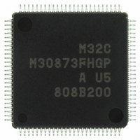
M30873FHGP#U5 Renesas Electronics America, M30873FHGP#U5 Datasheet - Page 335

M30873FHGP#U5
Manufacturer Part Number
M30873FHGP#U5
Description
IC M32C/87 MCU FLASH 100LQFP
Manufacturer
Renesas Electronics America
Series
M16C™ M32C/80r
Datasheet
1.M3087BFLGPU3.pdf
(629 pages)
Specifications of M30873FHGP#U5
Core Processor
M32C/80
Core Size
16/32-Bit
Speed
32MHz
Connectivity
CAN, EBI/EMI, I²C, IEBus, IrDA, SIO, UART/USART
Peripherals
DMA, POR, PWM, WDT
Number Of I /o
85
Program Memory Size
384KB (384K x 8)
Program Memory Type
FLASH
Ram Size
24K x 8
Voltage - Supply (vcc/vdd)
3 V ~ 5.5 V
Data Converters
A/D 26x10b; D/A 2x8b
Oscillator Type
Internal
Operating Temperature
-20°C ~ 85°C
Package / Case
100-LQFP
For Use With
R0K330879S001BE - KIT DEV RSK M32C/87R0K330879S000BE - KIT DEV RSK M32C/87
Lead Free Status / RoHS Status
Lead free / RoHS Compliant
Eeprom Size
-
Available stocks
Company
Part Number
Manufacturer
Quantity
Price
Part Number:
M30873FHGP#U5M30873FHGP#U3
Manufacturer:
Renesas Electronics America
Quantity:
10 000
- Current page: 335 of 629
- Download datasheet (16Mb)
M32C/87 Group (M32C/87, M32C/87A, M32C/87B)
REJ09B0180-0151 Rev.1.51 Jul 31, 2008
Page 311 of 587
18.3
18.4
Use the following procedure to read the AD0i register by a program.
•
•
To take full advantage of the A/D converter performance, Internal capacitor (C) charge shown in Figure 18.9
must be completed within the specified period (T) as sampling time. Output impedance of the sensor equivalent
circuit (R0) is determined by the following equation:
where:
Figure 18.9 shows a connection example of analog input pin and external sensor equivalent circuit.
In the following example, the impedance R0 is obtained from the equation above when VC changes from 0 to
VIN-(1/1024)VIN within the time (T), if the difference between VIN and VC becomes 1LSB. (1/1024) means
that A/D accuracy drop, due to insufficient capacitor charge, is held to 1LSB at time of A/D conversion in the
10-bit mode. Actual error, however, is the value of absolute accuracy added to 1LSB.
When φAD = 10 MHz, T = 0.3 μs in A/D conversion with the sample and hold function. Output impedance
(R0) enough to complete charging the capacitor (C) within the time (T) is determined by the following
equation:
Thus, the allowable output impedance R0 of the sensor equivalent circuit, making the accuracy (error) 1LSB or
less, is approximately 2.8 kΩ maximum.
In one-shot mode and single sweep mode:
Ensure that the A/D conversion is completed before reading the corresponding AD0i register. The IR bit in the
AD0IC register becomes 1 when the A/D conversion is completed.
In repeat mode, repeat sweep mode 0, and repeat sweep mode 1:
Read the AD0i register after setting the CPU clock as follows.
Read from the AD0i Register (i = 0 to 7)
(1) Set the PM24 bit in the PM2 register to 0 (clock selected by the CM07 bit).
(2) Set the CM07 bit in the CM0 register to 0 (clock selected by the CM21 bit divided by the MCD
(3) Set the MCD register to 12h (no division).
Output Impedance of Sensor Equivalent Circuit under A/D Conversion
When t = T,
Using T = 0.3 μs, R = 2.0 kΩ, C = 9.0 pF, X = 1, Y = 1024,
VC = Internal capacitor voltage
R = Internal resistance of the MCU
X = Accuracy (error) of the A/D converter
Y = Resolution (1024 in 10-bit mode, and 256 in 8-bit mode)
register).
R0
=
–
–
----------------------------------------------------
9.0
e
--------------------------- - T
C R0
R0
–
(
--------------------------- - T
C R0
VC
×
VC
(
=
0.3 10
1
10
1
+
–
+
=
–
=
R
×
------------- -
C
12
R
VIN
)
)
ln
T
⋅
VIN 1 e
X
--- -
Y
ln
–
=
=
6
------------ -
1024
–
–
X
--- -
Y
⎧
⎨
⎩
ln
R
X
--- - VIN
Y
1
X
--- -
Y
–
–
–
2.0 10
--------------------------- -t
C R0
=
(
×
VIN 1 X
1
+
R
⎛
⎝
3
)
⎫
⎬
⎭
≅
–
--- -
Y
2.8 10
⎞
⎠
×
3
Ω
18. A/D Converter
Related parts for M30873FHGP#U5
Image
Part Number
Description
Manufacturer
Datasheet
Request
R

Part Number:
Description:
KIT STARTER FOR M16C/29
Manufacturer:
Renesas Electronics America
Datasheet:

Part Number:
Description:
KIT STARTER FOR R8C/2D
Manufacturer:
Renesas Electronics America
Datasheet:

Part Number:
Description:
R0K33062P STARTER KIT
Manufacturer:
Renesas Electronics America
Datasheet:

Part Number:
Description:
KIT STARTER FOR R8C/23 E8A
Manufacturer:
Renesas Electronics America
Datasheet:

Part Number:
Description:
KIT STARTER FOR R8C/25
Manufacturer:
Renesas Electronics America
Datasheet:

Part Number:
Description:
KIT STARTER H8S2456 SHARPE DSPLY
Manufacturer:
Renesas Electronics America
Datasheet:

Part Number:
Description:
KIT STARTER FOR R8C38C
Manufacturer:
Renesas Electronics America
Datasheet:

Part Number:
Description:
KIT STARTER FOR R8C35C
Manufacturer:
Renesas Electronics America
Datasheet:

Part Number:
Description:
KIT STARTER FOR R8CL3AC+LCD APPS
Manufacturer:
Renesas Electronics America
Datasheet:

Part Number:
Description:
KIT STARTER FOR RX610
Manufacturer:
Renesas Electronics America
Datasheet:

Part Number:
Description:
KIT STARTER FOR R32C/118
Manufacturer:
Renesas Electronics America
Datasheet:

Part Number:
Description:
KIT DEV RSK-R8C/26-29
Manufacturer:
Renesas Electronics America
Datasheet:

Part Number:
Description:
KIT STARTER FOR SH7124
Manufacturer:
Renesas Electronics America
Datasheet:

Part Number:
Description:
KIT STARTER FOR H8SX/1622
Manufacturer:
Renesas Electronics America
Datasheet:

Part Number:
Description:
KIT DEV FOR SH7203
Manufacturer:
Renesas Electronics America
Datasheet:


