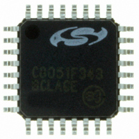
C8051F343-GQ Silicon Laboratories Inc, C8051F343-GQ Datasheet - Page 115

C8051F343-GQ
Manufacturer Part Number
C8051F343-GQ
Description
IC 8051 MCU FLASH 32K 32LQFP
Manufacturer
Silicon Laboratories Inc
Series
C8051F34xr
Specifications of C8051F343-GQ
Program Memory Type
FLASH
Program Memory Size
32KB (32K x 8)
Package / Case
32-LQFP
Core Processor
8051
Core Size
8-Bit
Speed
48MHz
Connectivity
SMBus (2-Wire/I²C), SPI, UART/USART, USB
Peripherals
Brown-out Detect/Reset, POR, PWM, Temp Sensor, WDT
Number Of I /o
25
Ram Size
2.25K x 8
Voltage - Supply (vcc/vdd)
2.7 V ~ 3.6 V
Data Converters
A/D 21x10b
Oscillator Type
Internal
Operating Temperature
-40°C ~ 85°C
Processor Series
C8051F3x
Core
8051
Data Bus Width
8 bit
Data Ram Size
2304 B
Interface Type
I2C, SMBus, SPI, UART, USB
Maximum Clock Frequency
48 MHz
Number Of Programmable I/os
25
Number Of Timers
4
Operating Supply Voltage
2.7 V to 5.25 V
Maximum Operating Temperature
+ 85 C
Mounting Style
SMD/SMT
3rd Party Development Tools
KSK-SL-F34X, KSK-SL-TOOLSTICK, PK51, CA51, A51, ULINK2
Development Tools By Supplier
C8051F340DK
Minimum Operating Temperature
- 40 C
On-chip Adc
10 bit, 17 Channel
Package
32LQFP
Device Core
8051
Family Name
C8051F34x
Maximum Speed
48 MHz
Data Rom Size
128 B
A/d Bit Size
10 bit
A/d Channels Available
17
Height
1.4 mm
Length
7 mm
Supply Voltage (max)
3.6 V
Supply Voltage (min)
2.7 V
Width
7 mm
Lead Free Status / RoHS Status
Lead free / RoHS Compliant
For Use With
336-1748 - ADAPTER TOOLSTICK FOR C8051F34X770-1006 - ISP 4PORT FOR SILABS C8051F MCU
Eeprom Size
-
Lead Free Status / Rohs Status
Lead free / RoHS Compliant
Other names
336-1301
Available stocks
Company
Part Number
Manufacturer
Quantity
Price
Company:
Part Number:
C8051F343-GQ
Manufacturer:
Silicon Laboratories Inc
Quantity:
10 000
Company:
Part Number:
C8051F343-GQR
Manufacturer:
Silicon Laboratories Inc
Quantity:
10 000
- Current page: 115 of 276
- Download datasheet (2Mb)
13.2. Accessing USB FIFO Space
The C8051F34x devices include 1k of RAM which functions as USB FIFO space. Figure 13.1 shows an
expanded view of the FIFO space and user XRAM. FIFO space is normally accessed via USB FIFO regis-
ters; see
FIFOs. The MOVX instruction should not be used to load or modify USB data in the FIFO space.
Unused areas of the USB FIFO space may be used as general purpose XRAM if necessary. The FIFO
block operates on the USB clock domain; thus the USB clock must be active when accessing FIFO space.
Note that the number of SYSCLK cycles required by the MOVX instruction is increased when accessing
USB FIFO space.
To access the FIFO RAM directly using MOVX instructions, the following conditions must be met: (1) the
USBFAE bit in register EMI0CF must be set to '1', and (2) the USB clock must be greater than or equal to
twice the SYSCLK (USBCLK > 2 x SYSCLK). When this bit is set, the USB FIFO space is mapped into
XRAM space at addresses 0x0400 to 0x07FF. The normal XRAM (on-chip or external) at the same
addresses cannot be accessed when the USBFAE bit is set to ‘1’.
Important Note: The USB clock must be active when accessing FIFO space.
Figure 13.1. USB FIFO Space and XRAM Memory Map with USBFAE set to ‘1’
Section “16.5. FIFO Management” on page 167
0xFFFF
0x07FF
0x07C0
0x07BF
0x03FF
0x073F
0x063F
0x043F
0x0800
0x0740
0x0640
0x0440
0x0400
0x0000
C8051F340/1/2/3/4/5/6/7/8/9/A/B/C/D
On/Off-Chip XRAM
On/Off-Chip XRAM
(128 bytes)
(256 bytes)
(512 bytes)
Endpoint0
Endpoint1
Endpoint2
Endpoint3
(64 bytes)
(64 bytes)
Free
Rev. 1.3
USB FIFO Space
(USB Clock Domain)
for more information on accessing these
115
Related parts for C8051F343-GQ
Image
Part Number
Description
Manufacturer
Datasheet
Request
R
Part Number:
Description:
SMD/C°/SINGLE-ENDED OUTPUT SILICON OSCILLATOR
Manufacturer:
Silicon Laboratories Inc
Part Number:
Description:
Manufacturer:
Silicon Laboratories Inc
Datasheet:
Part Number:
Description:
N/A N/A/SI4010 AES KEYFOB DEMO WITH LCD RX
Manufacturer:
Silicon Laboratories Inc
Datasheet:
Part Number:
Description:
N/A N/A/SI4010 SIMPLIFIED KEY FOB DEMO WITH LED RX
Manufacturer:
Silicon Laboratories Inc
Datasheet:
Part Number:
Description:
N/A/-40 TO 85 OC/EZLINK MODULE; F930/4432 HIGH BAND (REV E/B1)
Manufacturer:
Silicon Laboratories Inc
Part Number:
Description:
EZLink Module; F930/4432 Low Band (rev e/B1)
Manufacturer:
Silicon Laboratories Inc
Part Number:
Description:
I°/4460 10 DBM RADIO TEST CARD 434 MHZ
Manufacturer:
Silicon Laboratories Inc
Part Number:
Description:
I°/4461 14 DBM RADIO TEST CARD 868 MHZ
Manufacturer:
Silicon Laboratories Inc
Part Number:
Description:
I°/4463 20 DBM RFSWITCH RADIO TEST CARD 460 MHZ
Manufacturer:
Silicon Laboratories Inc
Part Number:
Description:
I°/4463 20 DBM RADIO TEST CARD 868 MHZ
Manufacturer:
Silicon Laboratories Inc
Part Number:
Description:
I°/4463 27 DBM RADIO TEST CARD 868 MHZ
Manufacturer:
Silicon Laboratories Inc
Part Number:
Description:
I°/4463 SKYWORKS 30 DBM RADIO TEST CARD 915 MHZ
Manufacturer:
Silicon Laboratories Inc
Part Number:
Description:
N/A N/A/-40 TO 85 OC/4463 RFMD 30 DBM RADIO TEST CARD 915 MHZ
Manufacturer:
Silicon Laboratories Inc
Part Number:
Description:
I°/4463 20 DBM RADIO TEST CARD 169 MHZ
Manufacturer:
Silicon Laboratories Inc


