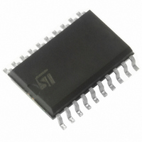
ST62T10CM6 STMicroelectronics, ST62T10CM6 Datasheet - Page 65

ST62T10CM6
Manufacturer Part Number
ST62T10CM6
Description
IC MCU 8BIT OTP 2K 20 SOIC
Manufacturer
STMicroelectronics
Series
ST6r
Datasheet
1.ST62T10CB6.pdf
(104 pages)
Specifications of ST62T10CM6
Core Processor
ST6
Core Size
8-Bit
Speed
8MHz
Peripherals
LVD, POR, WDT
Number Of I /o
12
Program Memory Size
2KB (2K x 8)
Program Memory Type
OTP
Ram Size
64 x 8
Voltage - Supply (vcc/vdd)
3 V ~ 6 V
Data Converters
A/D 8x8b
Oscillator Type
Internal
Operating Temperature
-40°C ~ 85°C
Package / Case
20-SOIC (7.5mm Width)
Cpu Family
ST6
Device Core Size
8b
Frequency (max)
8MHz
Total Internal Ram Size
64Byte
# I/os (max)
12
Number Of Timers - General Purpose
1
Operating Supply Voltage (typ)
3.3/5V
Operating Supply Voltage (max)
6V
Operating Supply Voltage (min)
3V
On-chip Adc
8-chx8-bit
Instruction Set Architecture
CISC
Operating Temp Range
-40C to 85C
Operating Temperature Classification
Industrial
Mounting
Surface Mount
Pin Count
20
Package Type
SOP
Processor Series
ST62T1x
Core
ST6
Data Bus Width
8 bit
Data Ram Size
64 B
Maximum Clock Frequency
8 MHz
Number Of Programmable I/os
12
Number Of Timers
1
Operating Supply Voltage
3 V to 6 V
Maximum Operating Temperature
+ 85 C
Mounting Style
SMD/SMT
Development Tools By Supplier
ST622XC-KIT/110, ST62GP-EMU2, ST62E2XC-EPB/110, ST62E6XC-EPB/US, STREALIZER-II
Minimum Operating Temperature
- 40 C
Controller Family/series
ST6
No. Of I/o's
12
Ram Memory Size
64Byte
Cpu Speed
8MHz
No. Of Timers
1
Rohs Compliant
Yes
Lead Free Status / RoHS Status
Lead free / RoHS Compliant
Eeprom Size
-
Connectivity
-
Lead Free Status / Rohs Status
Compliant
Other names
497-2097-5
Available stocks
Company
Part Number
Manufacturer
Quantity
Price
Part Number:
ST62T10CM6
Manufacturer:
ST
Quantity:
20 000
OPERATING CONDITIONS (Cont’d)
10.3.2 Operating Conditions with Low Voltage Detector (LVD)
Subject to general operating conditions for V
Notes:
1. LVD typical data are based on T
2. The minimum V
3. Data based on characterization results, not tested in production.
Figure 39. LVD Threshold Versus V
Figure 40. Typical LVD Thresholds Versus
Temperature for OTP devices
DEVICE UNDER
V
V
V
Vt
t
Thresholds [V]
4.2
3.8
3.6
g(VDD)
Symbol
IT+
IT-
hys
IN THIS AREA
4
POR
-40°C
RESET
f
OSC
Reset release threshold
(V
Reset generation threshold
(V
LVD voltage threshold hysteresis
V
Filtered glitch delay on V
DD
DD
DD
8
4
0
[MHz]
2.5
rise time rate
DD
rise)
fall)
25°C
rise time rate is needed to insure a correct device power-on and LVD reset. Not tested in production.
Parameter
T [°C]
3
2)
A
95°C
=25°C. They are given only as design guidelines and are not tested.
DD
3.5
3)
V
V
Vdd up
Vdd down
IT+
IT-
DD
V
IT-
≥3.6
and f
125°C
V
Not detected by the LVD
DD
4
IT+
OSC
, f
-V
OSC
IT-
3)
Conditions
, and T
Figure
Temperature for ROM devices
4.5
Thresholds [V]
4.2
3.8
3.6
4
-40°C
ST6208C/ST6209C/ST6210C/ST6220C
A
.
41.
5
Typical
25°C
Min
3.9
3.6
5.5
50
T [°C]
LVD
Typ
4.1
3.8
300
30
6
1)
95°C
thresholds
FUNCTIONALITY
NOT GUARANTEED
IN THIS AREA
FUNCTIONAL AREA
SUPPLY
VOLTAGE [V]
Max
4.3
700
V
V
4
Vdd up
Vdd down
IT+
IT-
125°C
mV/s
Unit
65/104
mV
ns
V
vs.
1


