ST7FOXK1T6TR STMicroelectronics, ST7FOXK1T6TR Datasheet
ST7FOXK1T6TR
Specifications of ST7FOXK1T6TR
Available stocks


Related parts for ST7FOXK1T6TR


ST7FOXK1T6TR Summary of contents
Page 1
Features Memories – Kbytes single voltage extended Flash (XFlash) Program memory with Read-Out Protection In-Circuit Programming and In-Application programming (ICP and IAP) Endurance: 1K write/erase cycles guaranteed Data retention: 20 years at 55 °C – 384 bytes ...
Page 2
Contents Contents 1 Description . . . . . . . . . . . . . . . . . . . . . . . . . . . . . . . . . . . . ...
Page 3
ST7FOXF1, ST7FOXK1, ST7FOXK2 6.2 Multi-oscillator (MO ...
Page 4
Contents 8.4 Active-halt and halt modes . . . . . . . . . . . . . . . . . . . . . . . . . . . . . . . . . . ...
Page 5
ST7FOXF1, ST7FOXK1, ST7FOXK2 10.2.5 10.2.6 10.3 Lite timer 2 (LT2 ...
Page 6
Contents 10.6.9 10.7 10-bit A/D converter (ADC ...
Page 7
ST7FOXF1, ST7FOXK1, ST7FOXK2 12.5 Communication interface characteristics . . . . . . . . . . . . . . . . . . . . . . . . 194 12.5.1 12.5.2 12.6 Clock and timing characteristics . ...
Page 8
List of tables List of tables Table 1. Device summary . . . . . . . . . . . . . . . . . . . . . . . . . . . . . . ...
Page 9
ST7FOXF1, ST7FOXK1, ST7FOXK2 2 Table 49 register mapping and reset values . . . . . . . . . . . . . . . . . . . . . . . . . . . ...
Page 10
List of tables Table 101. Thermal characteristics ...
Page 11
ST7FOXF1, ST7FOXK1, ST7FOXK2 List of figures Figure 1. General block diagram . . . . . . . . . . . . . . . . . . . . . . . . . . . . . ...
Page 12
List of figures Figure 49. One pulse mode and PWM timing diagram . . . . . . . . . . . . . . . . . . . . . . . . . . . . ...
Page 13
ST7FOXF1, ST7FOXK1, ST7FOXK2 1 Description The ST7FOX is a member of the ST7 microcontroller family. All ST7 devices are based on a common industry-standard 8-bit core, featuring an enhanced instruction set. The device is positioned at the entry level of ...
Page 14
Description Figure 1. General block diagram CLKIN OSC1 OSC2 RESET Note 1 : available on 8K version only 14/226 / 2 Ext. OSC 1 MHz / 2 to Internal 16 MHz clock Int. 8 MHz RC ...
Page 15
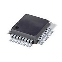
ST7FOXF1, ST7FOXK1, ST7FOXK2 2 Pin description Figure 2. 32-pin SDIP package pinout OCMP1_A ATPWM2/MCO/PA4(HS) Note 1: Available on 8K version only Figure 3. 32-pin LQFP 7x7 package pinout ATPWM1/PA3(HS) ATPWM2/MCO/PA4(HS) ATPWM3/PA5(HS) I2CDATA/PA6(HS) I2CCLK/PA7(HS) BREAK1/PC7 1 ei2 1) /PA0(HS) 2 ei2 ...
Page 16
Pin description Legend / Abbreviations for Type input output supply In/Output level: C Output level high sink (on N-buffer only) Port and control configuration: Input: float = floating, wpu = ...
Page 17
ST7FOXF1, ST7FOXK1, ST7FOXK2 Table 2. Device pin description (32-pin packages) (continued) Pin number Pin name 14 18 PB0/AIN0 15 19 PB1/AIN1/CLKIN 16 20 PB2/AIN2 ( PB3/AIN3/MOSI ( PB4/AIN4/MISO PB5/AIN5 (2) EXTCLK_A ( ...
Page 18
Pin description Table 2. Device pin description (32-pin packages) (continued) Pin number Pin name PA0 30 2 (5) (2) (HS) /OCMP1_A 31 3 PA1 (HS)/ATIC 32 4 PA2 (HS)/ATPWM0 1. In the open-drain output column, T defines a true open-drain ...
Page 19
ST7FOXF1, ST7FOXK1, ST7FOXK2 Table 3. Device pin description (20-pin package) Pin Pin Name Number 1 PC6 2 PA1 (HS)/ATIC 3 PA2 (HS)/ATPWM0 4 PA3 (HS)/ATPWM1 PA4 5 (HS)ATPWM2/MCO 6 PA5 (HS)ATPWM3 7 PA6 (HS)/I2CDATA 8 PA7 (HS)/ I2CCLK 9 RESET ...
Page 20
Register and memory mapping 3 Register and memory mapping As shown in Figure registers. The available memory locations consist of 128 bytes of register locations, 384 bytes of RAM and Kbytes of Flash program memory. The RAM ...
Page 21
ST7FOXF1, ST7FOXK1, ST7FOXK2 Table 4. Hardware register map Address Block Register label 0000h PADR 0001h Port A PADDR 0002h PAOR 0003h PBDR 0004h Port B PBDDR 0005h PBOR 0006h PCDR 0007h Port C PCDDR 0008h PCOR 0009h to 000Bh 000Ch ...
Page 22
Register and memory mapping Table 4. Hardware register map Address Block Register label 002Dh ISPR0 002Eh ISPR1 002Fh ITC ISPR2 0030h ISPR3 0031h EICR 0032h 0033h WDG WDGCR 0034h FLASH FCSR RC 0035h RCC_CSR Calibration 0036h ADCCSR 0037h ADC ADCDRH ...
Page 23
ST7FOXF1, ST7FOXK1, ST7FOXK2 Table 4. Hardware register map Address Block Register label TACR2 0055h TACR1 0056h TACSR 0057h TAICHR1 0058h TAICLR1 0059h TAOCHR1 005Ah TAOCLR1 005Bh 16-bit TACHR 005Ch (4) Timer TACLR 005Dh TAACHR 005Eh TAACLR 005Fh 0060h TAICHR2 0061h ...
Page 24
Flash programmable memory 4 Flash programmable memory 4.1 Introduction The ST7 single voltage extended Flash (XFlash non-volatile memory that can be electrically erased and programmed either on a byte-by-byte basis bytes in parallel. The ...
Page 25
ST7FOXF1, ST7FOXK1, ST7FOXK2 Depending on the ICP Driver code downloaded in RAM, Flash memory programming can be fully customized (number of bytes to program, program locations, or selection of the serial communication interface for downloading). 4.3.2 In Application Programming (IAP) ...
Page 26
Flash programmable memory during a reset. In the application, even if the pin is configured as output, any reset will put it back in input pull-up. Figure 6. Typical ICC Interface (See Note 3) APPLICATION POWER SUPPLY 26/226 ST7FOXF1, ST7FOXK1, ...
Page 27
ST7FOXF1, ST7FOXK1, ST7FOXK2 4.5 Memory protection There are two different types of memory protection: Read-Out Protection and Write/Erase Protection which can be applied individually. 4.5.1 Read-out protection Read-Out Protection, when selected provides a protection against program memory content extraction and ...
Page 28
Flash programmable memory 4.7 Description of Flash Control/Status register (FCSR) This register controls the XFlash erasing and programming using ICP, IAP or other programming methods. 1st RASS Key: 0101 0110 (56h) 2nd RASS Key: 1010 1110 (AEh) When an EPB ...
Page 29
ST7FOXF1, ST7FOXK1, ST7FOXK2 5 Central processing unit 5.1 Introduction This CPU has a full 8-bit architecture and contains six internal registers allowing efficient 8- bit data manipulation. 5.2 Main features 63 basic instructions Fast 8-bit by 8-bit multiply 17 main ...
Page 30
Central processing unit 5.3.1 Accumulator (A) The Accumulator is an 8-bit general purpose register used to hold operands and the results of the arithmetic and logic calculations and to manipulate data. 5.3.2 Index registers (X and Y) In indexed addressing ...
Page 31
ST7FOXF1, ST7FOXK1, ST7FOXK2 Bit Interrupt mask bit This bit is set by hardware when entering in interrupt or by software to disable all interrupts except the TRAP software interrupt. This bit is cleared by software. 0: Interrupts ...
Page 32
Central processing unit * Table 6. Interrupt software priority truth table 5.3.5 Stack Pointer (SP) Reset value: 01FFh The Stack Pointer is a 16-bit register which is always pointing to the next free location in the ...
Page 33
ST7FOXF1, ST7FOXK1, ST7FOXK2 Figure 8. Stack manipulation example CALL Subroutine @ 0180h SP SP PCH @ 01FFh PCL Stack Higher Address = 01FFh Stack Lower Address = 0180h PUSH Y POP Y Interrupt Event ...
Page 34
Supply, reset and clock management 6 Supply, reset and clock management The device includes a range of utility features for securing the application in critical situations (for example in case of a power brown-out), and reducing the number of external ...
Page 35
ST7FOXF1, ST7FOXK1, ST7FOXK2 These bytes are systematically programmed by ST. 6.1.2 Customized RC calibration If the application requires a higher frequency accuracy or if the voltage or temperature conditions change in the application, the frequency may need to be recalibrated. ...
Page 36
Supply, reset and clock management If a programming cycle is interrupted (by a RESET action), the integrity of the data in memory will not be guaranteed. Caution: When the Read-Out Protection is enabled through an option bit (see bytes), these ...
Page 37
ST7FOXF1, ST7FOXK1, ST7FOXK2 Case 2 Switching from AWU RC to internal RC 1. Reset the RC/AWU bit to enable the internal RC oscillator 2. Using a 4-bit counter, wait until 8 internal RC cycles have elapsed. The counter is running ...
Page 38
Supply, reset and clock management Figure 12. Clock management block diagram CK2 CK1 CR9 CR8 Prescaler CLKSEL[1:0] Option bits CLKIN CLKIN CLKIN CLKIN OSC /OSC1 1-16 MHz or 32kHz OSC2 f OSC /32 DIVIDER 6.2 Multi-oscillator (MO) The main clock ...
Page 39
ST7FOXF1, ST7FOXK1, ST7FOXK2 6.2.1 External clock source In this external clock mode, a clock signal (square, sinus or triangle) with ~50% duty cycle has to drive the OSC1 pin while the OSC2 pin is tied to ground. Note: When the ...
Page 40
Supply, reset and clock management Table 8. ST7 clock sources 6.3 Reset sequence manager (RSM) 6.3.1 Introduction The reset sequence manager includes three RESET sources as shown in External RESET source pulse Internal LVD RESET (Low Voltage Detection) Internal WATCHDOG ...
Page 41
ST7FOXF1, ST7FOXK1, ST7FOXK2 Table 9. CPU clock delay during Reset sequence External clock (connected to CLKIN/PB1 pin) External Crystal/Ceramic Oscillator (connected to OSC1/OSC2 pins) External Crystal/Ceramic 1-16 MHz Oscillator External Crystal/Ceramic 32 kHz Oscillator Figure 13. Reset sequence phases Clock ...
Page 42
Supply, reset and clock management 6.3.2 Asynchronous external RESET pin The RESET pin is both an input and an open-drain output with integrated R resistor. This pull-up has no fixed value but varies in accordance with the input voltage. It ...
Page 43
ST7FOXF1, ST7FOXK1, ST7FOXK2 6.3.5 Internal watchdog reset The Reset sequence generated by an internal watchdog counter overflow is shown in Figure 15: Reset sequences Starting from the watchdog counter underflow, the device RESET pin acts as an output that is ...
Page 44
Supply, reset and clock management 6.4 System Integrity management (SI) The System Integrity Management block contains the Low voltage Detector (LVD). Note: A reset can also be triggered following the detection of an illegal opcode or prebyte code. Refer to ...
Page 45
ST7FOXF1, ST7FOXK1, ST7FOXK2 Figure 16. Low voltage detector vs reset IT+(LVD) V IT-(LVD) RESET Figure 17. Reset and supply management block diagram RESET SEQUENCE RESET hys WATCHDOG TIMER (WDG) SYSTEM INTEGRITY MANAGEMENT ...
Page 46
Supply, reset and clock management 6.5 Register description 6.5.1 RC calibration control/status register (RCC_CSR) Reset value: 0000 0000 (00h Bits 7:2 = Reserved, forced by hardware Read mode 1: Write mode Bit 1 = ...
Page 47
ST7FOXF1, ST7FOXK1, ST7FOXK2 6.5.3 RC Control Register High (RCCRH) Reset value: 1111 1111 (FFh) 7 CR9 CR8 Bits 7:0 = CR[9:2] RC Oscillator Frequency Adjustment bits These bits must be written immediately after reset to adjust the RC oscillator frequency. ...
Page 48
Supply, reset and clock management 6.5.4 RC Control Register Low (RCCRL) Reset value: 011x 0x00 (xxh CR1 Bit 7 = Reserved, must be kept cleared Bits 6:5 = CR[1:0] RC Oscillator Frequency Adjustment bits These bits, as well ...
Page 49
ST7FOXF1, ST7FOXK1, ST7FOXK2 6.5.5 Prescaler register (PSCR) Reset value: 0000 0000 (00h) for ST7FOXF1 and ST7FOXK1 Reset value: 0000 0011 (03h) for ST7FOXK2 7 CK2 CK1 Bits 7:5 = CK[2:0] internal RC Prescaler Selection These bits are set by software ...
Page 50
Supply, reset and clock management Bit 2 = RC_FLAG RC Selection bit This bit is set and cleared by hardware switch from RC to AWU requested 1: RC clock activated and temporization completed Bit 1 = Reserved, must ...
Page 51
ST7FOXF1, ST7FOXK1, ST7FOXK2 7 Interrupts 7.1 Introduction The ST7 enhanced interrupt management provides the following features: Hardware interrupts Software interrupt (TRAP) Nested or concurrent interrupt management with flexible interrupt priority and level management: – software programmable nesting ...
Page 52
Interrupts Table 13. Interrupt software priority levels Interrupt software priority Level 0 (main) Level 1 Level 2 Level 3 (= interrupt disable) Figure 18. Interrupt processing flowchart RESET RESTORE PC FROM STACK 52/226 ST7FOXF1, ST7FOXK1, ST7FOXK2 Level ...
Page 53
ST7FOXF1, ST7FOXK1, ST7FOXK2 7.2.1 Servicing pending interrupts As several interrupts can be pending at the same time, the interrupt to be taken into account is determined by the following two-step process: The highest software priority interrupt is serviced, If several ...
Page 54
Interrupts Maskable sources Maskable interrupt vector sources can be serviced if the corresponding interrupt is enabled and if its own interrupt software priority (in ISPRx registers) is higher than the one currently being serviced (I1 and register). ...
Page 55
ST7FOXF1, ST7FOXK1, ST7FOXK2 7.4 Concurrent and nested management The following Figure 20 first is called concurrent mode and does not allow an interrupt to be interrupted, unlike the nested mode in Figure lowest to the highest: MAIN, IT5, IT4, IT3, ...
Page 56
Interrupts 7.5 Description of interrupt registers 7.5.1 CPU CC register interrupt bits Reset value: 111x 1010(xAh Bits I1, I0 Software Interrupt Priority bits These two bits indicate the current interrupt software priority (see These ...
Page 57
ST7FOXF1, ST7FOXK1, ST7FOXK2 The RESET and TRAP vectors have no software priorities. When one is serviced, the I1 and I0 bits of the CC register are both set. Level 0 cannot be written (I1_x = 1, I0_x = 0). In ...
Page 58
Interrupts Table 17. ST7FOXF1/ST7FOXK1 Interrupt mapping Source Number block RESET TRAP 0 AWU 1 2 ei0 External interrupt 0 (Port A) 3 ei1 External interrupt 1 (Port B) 4 ei2 External interrupt 2 (Port timer Output Compare ...
Page 59
ST7FOXF1, ST7FOXK1, ST7FOXK2 Table 18. ST7FOXK2 interrupt mapping Source Number block RESET TRAP 0 AWU ei0 External interrupt 0 (Port A) 5 ei1 External interrupt 1 (Port B) 6 ei2 External interrupt 2 (Port C) AT ...
Page 60
Interrupts 7.5.3 External Interrupt Control register (EICR) Reset value: 0000 0000 (00h Bits 7:6 = Reserved, must be kept cleared. Bits 5:4 = IS2[1:0] ei2 sensitivity bits These bits define the interrupt sensitivity for ei2 (Port C) ...
Page 61
ST7FOXF1, ST7FOXK1, ST7FOXK2 8 Power saving modes 8.1 Introduction To give a large measure of flexibility to the application in terms of power consumption, four main power saving modes are implemented in the ST7 (see Slow Wait (and Slow-Wait) Active ...
Page 62
Power saving modes 8.2 Slow mode This mode has two targets: To reduce power consumption by decreasing the internal clock in the device, To adapt the internal clock frequency (f Slow mode is controlled by the SMS bit in the ...
Page 63
ST7FOXF1, ST7FOXK1, ST7FOXK2 Figure 24. Wait mode flowchart 1. Before servicing an interrupt, the CC register is pushed on the stack. The I bit of the CC register is set during the interrupt routine and cleared when the CC register ...
Page 64
Power saving modes 8.4.1 Active-halt mode Active-Halt mode is the lowest power consumption mode of the MCU with a real-time clock available entered by executing the ‘HALT’ instruction when active halt mode is enabled. The MCU can exit ...
Page 65
ST7FOXF1, ST7FOXK1, ST7FOXK2 Figure 26. Active-halt mode flowchart 1. This delay occurs only if the MCU exits Active-Halt mode by means of a RESET. 2. Peripherals clocked with an external clock source can still be active. 3. Only the Lite ...
Page 66
Power saving modes Figure 27. Halt timing overview 1. A reset pulse of at least 42 µs must be applied when exiting from Halt mode. Figure 28. Halt mode flowchart 1. WDGHALT is an option bit. See option byte section ...
Page 67
ST7FOXF1, ST7FOXK1, ST7FOXK2 Halt mode recommendations Make sure that an external event is available to wake up the microcontroller from Halt mode. When using an external interrupt to wake up the microcontroller, reinitialize the corresponding I/O as “Input Pull-up with ...
Page 68
Power saving modes As soon as Halt mode is entered, and if the AWUEN bit has been set in the AWUCSR register, the AWU RC oscillator provides a clock signal (f a fixed divider and a programmable prescaler controlled by ...
Page 69
ST7FOXF1, ST7FOXK1, ST7FOXK2 Figure 31. AWUFH mode flowchart 1. WDGHALT is an option bit. See option byte section for more details. 2. Peripheral clocked with an external clock source can still be active. 3. Only an AWUFH interrupt and some ...
Page 70
Power saving modes 8.5.1 Register description 8.5.2 AWUFH Control/Status Register (AWUCSR) Reset value: 0000 0000 (00h Bits 7:3 = Reserved Bit 2 = AWUF Auto wakeup flag This bit is set by hardware when the AWU module ...
Page 71
ST7FOXF1, ST7FOXK1, ST7FOXK2 8.5.3 AWUFH prescaler register (AWUPR) Reset value: 1111 1111 (FFh) 7 AWUPR7 AWUPR6 Bits 7:0= AWUPR[7:0] Auto wakeup Prescaler These 8 bits define the AWUPR Dividing factor (see Table 21. Configuring the dividing factor AWUPR[7:0 00h 01h ...
Page 72
I/O ports 9 I/O ports 9.1 Introduction The I/O ports allow data transfer. An I/O port can contain pins. Each pin can be programmed independently either as a digital input or digital output. In addition, specific pins ...
Page 73
ST7FOXF1, ST7FOXK1, ST7FOXK2 Spurious interrupts When enabling/disabling an external interrupt by setting/resetting the related OR register bit, a spurious interrupt is generated if the pin level is low and its edge sensitivity includes falling/rising edge. This is due to the ...
Page 74
I/O ports 9.2.3 Alternate functions Many ST7s I/Os have one or more alternate functions. These may include output signals from, or input signals to, on-chip signals can be input/output to which ports. A signal coming from an on-chip peripheral can ...
Page 75
ST7FOXF1, ST7FOXK1, ST7FOXK2 Table 24. I/O port mode options Configuration mode Floating with/without Interrupt Input Pull-up with Interrupt Output Open Drain (logic level) 1. Off means implemented not activated, On means implemented and activated. Table 25. ST7FOXF1/ST7FOXK1/ST7FOXK2 I/O port configuration ...
Page 76
I/O ports 9.2.4 Analog alternate function Configure the I/O as floating input to use an ADC input. The analog multiplexer (controlled by the ADC registers) switches the analog voltage present on the selected pin to the common analog rail, connected ...
Page 77
ST7FOXF1, ST7FOXK1, ST7FOXK2 9.6 Interrupts The external interrupt event generates an interrupt if the corresponding configuration is selected with DDR and OR registers and if the I bit in the CC register is cleared (RIM instruction). Table 27. Description of ...
Page 78
I/O ports M Table 30. PC3 pin Table 31. Port configuration Port Pin name Port A Port B Port C Table 32. I/O port register mapping and reset values Address Register 7 label (Hex.) PADR MSB 0000h Reset Value 0 ...
Page 79
ST7FOXF1, ST7FOXK1, ST7FOXK2 10 On-chip peripherals 10.1 Watchdog timer (WDG) 10.1.1 Introduction The Watchdog timer is used to detect the occurrence of a software fault, usually generated by external interference or by unforeseen logical conditions, which causes the application program ...
Page 80
On-chip peripherals The application program must write in the CR register at regular intervals during normal operation to prevent an MCU reset. This downcounter is free-running: it counts down even if the watchdog is disabled. The value to be stored ...
Page 81
ST7FOXF1, ST7FOXK1, ST7FOXK2 10.1.6 Register description Control register (WDGCR) Reset value: 0111 1111 (7Fh) 7 WDGA Bit 7 = WDGA Activation bit This bit is set by software and only cleared by hardware after a reset. When WDGA = 1, ...
Page 82
On-chip peripherals 10.2 Dual 12-bit autoreload timer 10.2.1 Introduction The 12-bit Autoreload timer can be used for general-purpose timing functions based on one or two free-running 12-bit upcounters with an Input Capture register and four PWM output channels. ...
Page 83
ST7FOXF1, ST7FOXK1, ST7FOXK2 Figure 35. Single timer mode (ENCNTR2=0) ATIC Edge Detection Circuit 12-Bit Autoreload register 1 Clock Control Figure 36. Dual timer mode (ENCNTR2=1) Edge Detection Circuit ATIC 12-Bit Autoreload register 1 12-Bit Autoreload register 2 Control LTIC 12-bit ...
Page 84
On-chip peripherals 10.2.3 Functional description PWM mode This mode allows up to four Pulse Width Modulated signals to be generated on the PWMx output pins. PWM frequency The four PWM signals can have the same frequency (f frequencies. This is ...
Page 85
ST7FOXF1, ST7FOXK1, ST7FOXK2 Figure 37. PWM polarity inversion The Data Flip Flop (DFF) applies the polarity inversion when triggered by the counter overflow input. Output control The PWMx output signals can be enabled or disabled using the OEx bits in ...
Page 86
On-chip peripherals Figure 39. PWM signal from 0% to 100% duty cycle f COUNTER COUNTER DCRx=000h DCRx=FFDh DCRx=FFEh DCRx=000h Dead time generation A dead time can be inserted between PWM0 and PWM1 using the DTGR register. This is required for ...
Page 87
ST7FOXF1, ST7FOXK1, ST7FOXK2 Figure 40. Dead time generation CK_CNTR1 CNTR1 PWM 0 PWM 1 PWM 0 PWM 1 In the above example, when the DTE bit is set: PWM goes low at DCR0 match and goes high at ATR1+Tdt PWM1 ...
Page 88
On-chip peripherals When a break function is activated (BA bit =1 and BREN1/BREN2 =1): The break pattern (PWM[3:0] bits in the BREAKCR) is forced directly on the PWMx output pins if respective OEx is set. (after the inverter). The 12-bit ...
Page 89
ST7FOXF1, ST7FOXK1, ST7FOXK2 Figure 42. ST7FOXK2 Block diagram of break function BREAK1 pin Comparator1 BREAKCR2 register BR2SEL BR2EDGE BREAK2 pin Comparator2 Output compare mode To use this function, load a 12-bit value in the Preload DCRxH and DCRxL registers. When ...
Page 90
On-chip peripherals Figure 43. Block diagram of output compare mode (single timer) DCRx PRELOAD DUTY CYCLE REG0/1/2/3 (ATCSR2) TRAN1 (ATCSR) OVF CNTR1 Input capture mode The 12-bit ATICR register is used to latch the value of the 12-bit free running ...
Page 91
ST7FOXF1, ST7FOXK1, ST7FOXK2 Figure 45. Input capture timing diagram f COUNTER COUNTER1 01h ATIC PIN ICF FLAG Long range input capture Pulses that last more than 8 µs can be measured with an accuracy of 4 µ MHz ...
Page 92
On-chip peripherals Since the Input Capture flags (ICF) for both timers (AT4 timer and LT timer) are set when signal transition occurs, software must mask one interrupt by clearing the corresponding ICIE bit before setting the ICS bit. If the ...
Page 93
ST7FOXF1, ST7FOXK1, ST7FOXK2 Figure 47. Long range input capture timing diagram f OSC/32 TB Counter1 F9h CNTR1 LTIC LTICR ATICRH ATICRL 00h LT1 F9h 00h ATH1 & ATL1 00h LT1 0h ATH1 00h ATL1 On-chip peripherals _ ...
Page 94
On-chip peripherals One pulse mode One Pulse mode can be used to control PWM2/3 signal with an external LTIC pin. This mode is available only in Dual Timer mode i.e. only for CNTR2, when the OP_EN bit in PWM3CSR register ...
Page 95
ST7FOXF1, ST7FOXK1, ST7FOXK2 How to enter one pulse mode The steps required to enter One Pulse mode are the following: 1. Load ATR2H/ATR2L with required value. 2. Load DCR3H/DCR3L for PWM3. ATR2 value must be greater than DCR3. 3. Set ...
Page 96
On-chip peripherals Figure 50. Dynamic DCR2/3 update in one pulse mode f counter2 CNTR2 LTIC FORCE2 TRAN2 DCR2/3 PWM2/3 96/226 (DCR3) 000 FFF 000 old (DCR2/3) old extra PWM3 period due to DCR3 update dynamically in one-pulse mode. ST7FOXF1, ST7FOXK1, ...
Page 97
ST7FOXF1, ST7FOXK1, ST7FOXK2 Force update In order not to wait for the counter programmable counter which when set, make the counters start with the overflow value, i.e. FFFh. After overflow, the counters start counting from their respective auto reload register ...
Page 98
On-chip peripherals 10.2.6 Register description Timer control status register (ATCSR) Reset value: 0x00 0000 (x0h ICF Bit 7 = Reserved Bit 6 = ICF Input Capture flag This Bit is set by hardware and cleared by software by ...
Page 99
ST7FOXF1, ST7FOXK1, ST7FOXK2 Bit 0 = CMPIE Compare Interrupt Enable bit This bit is read/write by software and cleared by hardware after a reset. it can be used to mask the interrupt generated when any of the cmpfx bit is ...
Page 100
On-chip peripherals Autoreload register (ATR1H) Reset value: 0000 0000 (00h Autoreload register (ATR1L) Reset value: 0000 0000 (00h) 7 ATR7 ATR6 Bits 11:0 = ATR1[11:0] Autoreload register 1: This is a 12-bit register which is written by ...
Page 101
ST7FOXF1, ST7FOXK1, ST7FOXK2 This bit is read/write by software and cleared by hardware after a reset. This bit enables the One Pulse feature for PWM2 and PWM3 (only available for PWM3CSR) 0: One Pulse mode disable for PWM2/3. 1: One ...
Page 102
On-chip peripherals Bit 5 = BA1 Break 1 Active bit (BA on ST7FOXF1/ST7FOXK1) This bit is read/write by software, cleared by hardware after reset and set by hardware when the active level defined by the BR1EDGE bit is applied on ...
Page 103
ST7FOXF1, ST7FOXK1, ST7FOXK2 Break control register 2 (BREAKCR2) Reset value: 0000 0000 (00h) 7 BR2SEL BR2EDGE Note: This register is available on ST7FOXK2 only Bit 7 = BR2SEL Break 2 input selection bit This bit is read/write by software and ...
Page 104
On-chip peripherals PWMx Duty Cycle register High (DCRxH) Reset value: 0000 0000 (00h Bits 15:12 = Reserved. PWMx Duty Cycle register Low (DCRxL) Reset value: 0000 0000 (00h) 7 DCR7 DCR6 Bits 11:0 = DCRx[11:0] PWMx Duty ...
Page 105
ST7FOXF1, ST7FOXK1, ST7FOXK2 Input Capture register Low (ATICRL) Reset value: 0000 0000 (00h) 7 ICR7 ICR6 Bits 11:0 = ICR[11:0] Input Capture Data. This is a 12-bit register which is readable by software and cleared by hardware after a reset. ...
Page 106
On-chip peripherals Timer Control register 2 (ATCSR2) Reset value: 0000 0011 (03h) 7 FORCE2 FORCE1 Bit 7 = FORCE2 Force Counter 2 Overflow bit This bit is read/set by software. When set, it loads FFFh in the CNTR2 register. It ...
Page 107
ST7FOXF1, ST7FOXK1, ST7FOXK2 Bit 1= TRAN2 Transfer enable2 bit This bit is read/write by software, cleared by hardware after each completed transfer and set by hardware after reset. It controls the transfers on CNTR2. It allows the value of the ...
Page 108
On-chip peripherals Dead Time Generator register (DTGR) Reset value: 0000 0000 (00h) 7 DTE DT6 Bit 7 = DTE Dead Time Enable bit This bit is read/write by software. It enables a dead time generation on PWM0/PWM1 Dead ...
Page 109
ST7FOXF1, ST7FOXK1, ST7FOXK2 Table 38. Register mapping and reset values (continued) Add. Register 7 (Hex) label DCR0L DCR7 001C Reset Value 0 DCR1H 001D 0 Reset Value DCR1L DCR7 001E Reset Value 0 DCR2H 001F 0 Reset Value DCR2L DCR7 ...
Page 110
On-chip peripherals 10.3 Lite timer 2 (LT2) 10.3.1 Introduction The Lite timer can be used for general-purpose timing functions based on two free- running 8-bit upcounters, a watchdog function and an 8-bit Input Capture register. 10.3.2 Main features ...
Page 111
ST7FOXF1, ST7FOXK1, ST7FOXK2 Figure 52. Lite timer 2 block diagram f /32 OSC LTCNTR 8-bit TIMEBASE COUNTER 2 LTARR 8-bit AUTORELOAD REGISTER 8-bit TIMEBASE COUNTER 1 LTICR LTIC INPUT CAPTURE REGISTER 10.3.3 Functional description Timebase Counter 1 The 8-bit value ...
Page 112
On-chip peripherals Timebase Counter 2 Counter 8-bit autoreload upcounter. It can be read by accessing the LTCNTR register. After an MCU reset, it increments at a frequency of f stored in the LTARR register. A counter overflow ...
Page 113
ST7FOXF1, ST7FOXK1, ST7FOXK2 In this case, the HALT instruction stops the oscillator. When the oscillator is stopped, the Lite timer stops counting and is no longer able to generate a Watchdog reset until the microcontroller receives an external interrupt or ...
Page 114
On-chip peripherals 10.3.5 Interrupts Table 40. Description of interrupt events Interrupt Event Timebase 1 Event Timebase 2 Event IC Event The TBxF and ICF interrupt events are connected to separate interrupt vectors (see Section 7: Interrupts). They generate an interrupt ...
Page 115
ST7FOXF1, ST7FOXK1, ST7FOXK2 Lite Timer Autoreload register (LTARR) Reset value: 0000 0000 (00h) 7 AR7 AR6 Bits 7:0 = AR[7:0] Counter 2 Reload value These bits register is read/write by software. The LTARR value is automatically loaded into Counter 2 ...
Page 116
On-chip peripherals Bit Timebase period selection bit This bit is set and cleared by software. 0: Timebase period = t 1: Timebase period = t Bit 4 = TB1IE Timebase Interrupt enable bit This bit is set ...
Page 117
ST7FOXF1, ST7FOXK1, ST7FOXK2 10.4 16-bit timer 10.4.1 Introduction The timer consists of a 16-bit free-running counter driven by a programmable prescaler. It may be used for a variety of purposes, including pulse length measurement two input signals ...
Page 118
On-chip peripherals Counter register (CR) Counter high register (CHR) is the most significant byte (MSB). Counter low register (CLR) is the least significant byte (LSB). Alternate counter register (ACR) Alternate counter high register (ACHR) is the MSB. Alternate counter low ...
Page 119
ST7FOXF1, ST7FOXK1, ST7FOXK2 Figure 55. Timer block diagram f CPU 8 high EXEDG 1/2 1/4 1/8 EXTCLK pin CC[1:0] Overflow detect circuit ICF1 OCF1 TOF ICF2 CSR (control/status register ICIE OCIE TOIE FOLV2 (1) Timer interrupt 1. If IC, OC ...
Page 120
On-chip peripherals 16-bit read sequence (from either the counter register or the alternate counter register) Figure 56. 16-bit read sequence The user must read the MSB first, then the LSB value is buffered automatically. This buffered value remains unchanged until ...
Page 121
ST7FOXF1, ST7FOXK1, ST7FOXK2 A minimum of four falling edges of the CPU clock must occur between two consecutive active edges of the external clock; thus the external clock frequency must be less than a quarter of the CPU clock frequency. ...
Page 122
On-chip peripherals Input capture In this section, the index, i, may because there are two input capture functions in the 16-bit timer. The two input capture 16-bit registers (IC1R and IC2R) are used to latch the ...
Page 123
ST7FOXF1, ST7FOXK1, ST7FOXK2 the user toggle the output pin and if the ICIE bit is set. This can be avoided if the input capture function i is disabled by reading the ICiHR (see note 1). 6 The TOF bit can ...
Page 124
On-chip peripherals Output compare In this section, the index, i, may because there are two output compare functions in the 16-bit timer. This function can be used to control an output waveform or indicate when a ...
Page 125
ST7FOXF1, ST7FOXK1, ST7FOXK2 The OC R register value required for a specific timing application can be calculated using i the following formula: Equation 1 Where: ∆ output compare period (in seconds CPU clock frequency (in hertz) ...
Page 126
On-chip peripherals Forced compare output capability When the FOLVi bit is set by software, the OLVLi bit is copied to the OCMPi pin. The OLVi bit has to be toggled in order to toggle the OCMPi pin when it is ...
Page 127
ST7FOXF1, ST7FOXK1, ST7FOXK2 Figure 64. Output compare timing diagram, f Output compare register i (OCRi) Output compare flag i (OCFi) One pulse mode One pulse mode enables the generation of a pulse when an external event occurs. This mode is ...
Page 128
On-chip peripherals Figure 65. One pulse mode sequence When a valid event occurs on the ICAP1 pin, the counter value is loaded in the ICR1 register. The counter is then initialized to FFFCh, the OLVL2 bit is output on the ...
Page 129
ST7FOXF1, ST7FOXK1, ST7FOXK2 Note: 1 The OCF1 bit cannot be set by hardware in one pulse mode but the OCF2 bit can generate an output compare interrupt. 2 When the pulse width modulation (PWM) and one pulse mode (OPM) bits ...
Page 130
On-chip peripherals Note: There is a locking mechanism for transferring the OCiR value to the buffer. After a write to the OCiHR register, transfer of the new compare value to the buffer is inhibited until OCiLR is also written. Unlike ...
Page 131
ST7FOXF1, ST7FOXK1, ST7FOXK2 The OC R register value required for a specific timing application can be calculated using i the following formula: Equation 5 Where signal or pulse period (in seconds CPU clock frequency (in hertz) ...
Page 132
On-chip peripherals 10.4.5 Interrupts Table 43. 16-bit timer interrupt control/wakeup capability Input capture 1 event/counter reset in PWM mode Input capture 2 event Output compare 1 event (not available in PWM mode) Output compare 2 event (not available in PWM ...
Page 133
ST7FOXF1, ST7FOXK1, ST7FOXK2 10.4.7 16-bit timer registers Each timer is associated with three control and status registers, and with six pairs of data registers (16-bit values) relating to the two input captures, the two output compares, the counter and the ...
Page 134
On-chip peripherals Bit 1 = IEDG1 Input edge 1 This bit determines which type of level transition on the ICAP1 pin triggers the capture falling edge triggers the capture 1: A rising edge triggers the capture Bit 0 ...
Page 135
ST7FOXF1, ST7FOXK1, ST7FOXK2 10: Timer clock = f 11: Timer clock = external clock (where available) Note: If the external clock pin is not available, programming the external clock configuration stops the counter. Bit 1 = IEDG2 Input edge 2 ...
Page 136
On-chip peripherals Bit 4 = ICF2 Input capture flag input capture (reset value input capture has occurred on the ICAP2 pin. To clear this bit, first read the SR register, then read or write the ...
Page 137
ST7FOXF1, ST7FOXK1, ST7FOXK2 Timer A Output compare 1 high register (TAOC1HR) Reset value: 1000 0000 (80h) This is an 8-bit register that contains the high part of the value to be compared to the CHR register. 7 MSB Timer A ...
Page 138
On-chip peripherals Counter high register (CHR) Reset value: 1111 1111 (FFh) This is an 8-bit read-only register that contains the high part of the counter value. 7 MSB Counter low register (CLR) Reset value: 1111 1100 (FCh) This is an ...
Page 139
ST7FOXF1, ST7FOXK1, ST7FOXK2 Input capture 2 high register (IC2HR) Reset value: undefined This is an 8-bit read-only register that contains the high part of the counter value (transferred by the input capture 2 event). 7 MSB Input capture 2 low ...
Page 140
On-chip peripherals Table 45. 16-bit timer register map and reset values (continued) Address (Hex.) Register label TAACHR 5E Reset value TAACLR 5F Reset value TAICHR2 60 Reset value TAICLR2 61 Reset value TAOCHR2 62 Reset value TAOCLR2 63 Reset value ...
Page 141
ST7FOXF1, ST7FOXK1, ST7FOXK2 2 10 bus interface (I 10.5.1 Introduction 2 The I C Bus Interface serves as an interface between the microcontroller and the serial I bus. It provides both multimaster and slave functions, and controls all ...
Page 142
On-chip peripherals Mode selection The interface can operate in the four following modes: Slave transmitter/receiver Master transmitter/receiver By default, it operates in slave mode. The interface automatically switches from slave to master after it generates a START condition and from ...
Page 143
ST7FOXF1, ST7FOXK1, ST7FOXK2 2 When the I C cell is enabled, the SDA and SCL ports must be configured as floating inputs. In this case, the value of the external pull-up resistor used depends on the application. 2 When the ...
Page 144
On-chip peripherals 10.5.4 Functional description Refer to the CR, SR1 and SR2 registers default the I C interface operates in Slave mode (M/SL bit is cleared) except when it initiates a transmit or receive sequence. First the ...
Page 145
ST7FOXF1, ST7FOXK1, ST7FOXK2 Closing slave communication After the last data byte is transferred a Stop Condition is generated by the master. The interface detects this condition and sets: EVF and STOPF bits with an interrupt if the ITE bit is ...
Page 146
On-chip peripherals Master mode To switch from default Slave mode to Master mode a Start condition generation is needed. Start condition Setting the START bit while the BUSY bit is cleared causes the interface to switch to Master mode (M/SL ...
Page 147
ST7FOXF1, ST7FOXK1, ST7FOXK2 Master transmitter Following the address transmission and after SR1 register has been read, the master sends bytes from the DR register to the SDA line via the internal shift register. The master waits for a read of ...
Page 148
On-chip peripherals Figure 71. Transfer sequencing 7-bit slave receiver S Address A 7-bit slave transmitter S Address A 7-bit master receiver S Address A EV5 7-bit master transmitter S Address A EV5 10-bit slave receiver S Header A 10-bit slave ...
Page 149
ST7FOXF1, ST7FOXK1, ST7FOXK2 subsequent EV4 is not seen. 6. EV4: EVF=1, STOPF=1, cleared by reading SR2 register. 7. EV5: EVF=1, SB=1, cleared by reading SR1 register followed by writing DR register. 8. EV6: EVF=1, cleared by reading SR1 register followed ...
Page 150
On-chip peripherals 10.5.7 Register description Control register (I2CCR) Reset value: 0000 0000 (00h Bits 7:6 = Reserved. Forced hardware. Bit Peripheral Enable bit This bit is set and ...
Page 151
ST7FOXF1, ST7FOXK1, ST7FOXK2 Bit 1 = STOP Generation of a Stop condition bit This bit is set and cleared by software also cleared by hardware in master mode. Note: This bit is not cleared when the interface is ...
Page 152
On-chip peripherals Status register 1 (I2CSR1) Reset value: 0000 0000 (00h) 7 EVF ADD10 Bit 7 = EVF Event flag This bit is set by hardware as soon as an event occurs cleared by software ...
Page 153
ST7FOXF1, ST7FOXK1, ST7FOXK2 Bit 3 = BTF Byte Transfer Finished bit This bit is set by hardware as soon as a byte is correctly received or transmitted with interrupt generation if ITE= cleared by software reading SR1 register ...
Page 154
On-chip peripherals Status register 2 (I2CSR2) Reset value: 0000 0000 (00h Bits 7:5 = Reserved. Forced hardware. Bit Acknowledge failure bit This bit is set by hardware when ...
Page 155
ST7FOXF1, ST7FOXK1, ST7FOXK2 Note Bus Error occurs, a Stop or a repeated Start condition should be generated by the Master to re-synchronize communication, get the transmission acknowledged and the bus released for further communication Bit 0 = GCAL ...
Page 156
On-chip peripherals Own Address register (I2COAR1) Reset value: 0000 0000 (00h) 7 ADD7 ADD6 In 7-bit addressing mode Bits 7:1 = ADD[7:1] Interface address. These bits define the I interface. They are not cleared when the interface ...
Page 157
ST7FOXF1, ST7FOXK1, ST7FOXK2 2 Table 49 register mapping and reset values Address Register label (Hex.) I2CCR 0064h Reset Value I2CSR1 0065h Reset Value I2CSR2 0066h Reset Value I2CCCR 0067h Reset Value I2COAR1 0068h Reset Value I2COAR2 0069h Reset ...
Page 158
On-chip peripherals 10.6 Serial peripheral interface (SPI) 10.6.1 Introduction The Serial Peripheral Interface (SPI) allows full-duplex, synchronous, serial communication with external devices. An SPI system may consist of a master and one or more slaves or a system in which ...
Page 159
ST7FOXF1, ST7FOXK1, ST7FOXK2 Figure 73. Serial peripheral interface block diagram SPIDR Read Buffer MOSI MISO 8-Bit Shift Register SOD bit SCK SS 10.6.4 Functional description A basic example of interconnections between a single master and a single slave is illustrated ...
Page 160
On-chip peripherals Figure 74. Single master/ single slave application MASTER MSBit 8-BIT SHIFT REGISTER SPI CLOCK GENERATOR Slave select management As an alternative to using the SS pin to control the Slave Select signal, the application can choose to manage ...
Page 161
ST7FOXF1, ST7FOXK1, ST7FOXK2 Figure 75. Generic SS timing diagram MOSI/MISO Master SS Slave SS (if CPHA = 0) Slave SS (if CPHA = 1) Figure 76. Hardware/software slave select management Master mode operation In master mode, the serial clock is ...
Page 162
On-chip peripherals Master mode transmit sequence When software writes to the SPIDR register, the data byte is loaded into the 8-bit shift register and then shifted out serially to the MOSI pin most significant bit first. When data transfer is ...
Page 163
ST7FOXF1, ST7FOXK1, ST7FOXK2 The SPIF bit can be cleared during a second transmission; however, it must be cleared before the second SPIF bit in order to prevent an Overrun condition (see condition (OVR)). 10.6.5 Clock phase and clock polarity Four ...
Page 164
On-chip peripherals Figure 77. Data clock timing diagram SCK (CPOL = 1) SCK (CPOL = 0) MSBit MISO (from master) MSBit MOSI (from slave) SS (to slave) CAPTURE STROBE SCK (CPOL = 1) SCK (CPOL = 0) MISO MSBit (from ...
Page 165
ST7FOXF1, ST7FOXK1, ST7FOXK2 1. A read access to the SPICSR register while the MODF bit is set write to the SPICR register. Note: To avoid any conflicts in an application with multiple slaves, the SS pin must be ...
Page 166
On-chip peripherals Figure 78. Clearing the WCOL bit (write collision flag) software sequence Clearing sequence after SPIF = 1 (end of a data byte transfer) Read SPICSR 1st Step 2nd Step Read SPIDR Clearing sequence before SPIF = 1 (during ...
Page 167
ST7FOXF1, ST7FOXK1, ST7FOXK2 Figure 79. Single master / multiple slave configuration SCK MOSI MOSI SCK 5V SS 10.6.7 Low power modes Table 50. Low power mode descriptions Mode WAIT HALT 10.6.8 Interrupts Table 51. Interrupt events Interrupt event SPI End ...
Page 168
On-chip peripherals 10.6.9 Register description SPI Control register (SPICR) Reset value: 0000 xxxx (0xh) 7 SPIE SPE Bit 7 = SPIE Serial Peripheral interrupt enable. This bit is set and cleared by software. 0: Interrupt is inhibited 1: An SPI ...
Page 169
ST7FOXF1, ST7FOXK1, ST7FOXK2 Bit 2 = CPHA Clock phase. This bit is set and cleared by software. 0: The first clock transition is the first data capture edge. 1: The second clock transition is the first capture edge. The slave ...
Page 170
On-chip peripherals SPI control/status register (SPICSR) Reset Value: 0000 0000 (00h) 7 SPIF WCOL Bit 7 = SPIF Serial Peripheral Data Transfer Flag (Read only). This bit is set by hardware when a transfer has been completed. An interrupt is ...
Page 171
ST7FOXF1, ST7FOXK1, ST7FOXK2 Bit 1 = SSM SS Management. This bit is set and cleared by software. When set, it disables the alternate function of the SPI SS pin and uses the SSI bit value instead. See Section Slave select ...
Page 172
On-chip peripherals Table 53. SPI register map and reset values Address Register label (Hex.) SPIDR 70 Reset Value SPICR 71 Reset Value SPICSR 72 Reset Value 172/226 MSB SPIE SPE SPR2 MSTR ...
Page 173
ST7FOXF1, ST7FOXK1, ST7FOXK2 10.7 10-bit A/D converter (ADC) 10.7.1 Introduction The on-chip Analog to Digital Converter (ADC) peripheral is a 10-bit, successive approximation converter with internal sample and hold circuitry. This peripheral has multiplexed analog input channels ...
Page 174
On-chip peripherals Figure 80. ADC block diagram f CPU AIN0 AIN1 AINx Digital A/D conversion result The conversion is monotonic, meaning that the result never decreases if the analog input does not and never increases if the analog input does ...
Page 175
ST7FOXF1, ST7FOXK1, ST7FOXK2 Configuring the A/D conversion The analog input ports must be configured as input, no pull-up, no interrupt (see I/O ports). Using these pins as analog inputs does not affect the ability of the port to be read ...
Page 176
On-chip peripherals 10.7.6 Register description Control/status register (ADCCSR) Reset value: 0000 0000 (00h) 7 EOC SPEED Read only Bit 7 = EOC End of Conversion bit This bit is set by hardware cleared by hardware when software reads ...
Page 177
ST7FOXF1, ST7FOXK1, ST7FOXK2 Data register High (ADCDRH) Reset value: xxxx xxxx (xxh Bits 7:0 = D[9:2] MSB of Analog Converted Value ADC Control/data register Low (ADCDRL) Reset value: 0000 00xx (0xh Bits 7:4 = ...
Page 178
Instruction set 11 Instruction set 11.1 ST7 addressing modes The ST7 core features 17 different addressing modes which can be classified in seven main groups: Table 58. Description of addressing modes Addressing mode The ST7 instruction set is designed to ...
Page 179
ST7FOXF1, ST7FOXK1, ST7FOXK2 Table 59. ST7 addressing mode overview (continued) Mode Long Indirect Indexed Relative Direct Relative Indirect Bit Direct Bit Indirect Bit Direct Relative Bit Indirect Relative 1. At the time the instruction is executed, the Program Counter (PC) ...
Page 180
Instruction set Table 60. Instructions supporting inherent addressing mode (continued) SLL, SRL, SRA, RLC, RRC 11.1.2 Immediate mode Immediate instructions have 2 bytes, the first byte contains the opcode, the second byte contains the operand value. Imm Table 61. Instructions ...
Page 181
ST7FOXF1, ST7FOXK1, ST7FOXK2 Indexed mode (long) The offset is a word, thus allowing 64 Kbyte addressing space and requires 2 bytes after the opcode. 11.1.5 Indirect modes (short, long) The required data byte to do the operation is found by ...
Page 182
Instruction set Table 62. Instructions supporting direct, indexed, indirect and indirect indexed addressing modes (continued) Short instructions only SLL, SRL, SRA, RLC, RRC 11.1.7 Relative modes (direct, indirect) This addressing mode is used to modify the PC register value by ...
Page 183
ST7FOXF1, ST7FOXK1, ST7FOXK2 11.2 Instruction groups The ST7 family devices use an Instruction Set consisting of 63 instructions. The instructions may be subdivided into 13 main groups as illustrated in the following table: Table 64. ST7 instruction set Load and ...
Page 184
Instruction set 11.2.1 Illegal opcode reset In order to provide enhanced robustness to the device against unexpected behavior, a system of illegal opcode detection is implemented: a reset is generated if the code to be executed does not correspond to ...
Page 185
ST7FOXF1, ST7FOXK1, ST7FOXK2 Table 65. Illegal opcode detection (continued) Mnemo Description JRPL Jump (plus) JREQ Jump (equal) JRNE Jump (not equal) JRC Jump JRNC ...
Page 186
Instruction set Table 65. Illegal opcode detection (continued) Mnemo Description WFI Wait for Interrupt XOR Exclusive OR 186/226 Function/Example Dst XOR M A ST7FOXF1, ST7FOXK1, ST7FOXK2 Src ...
Page 187
ST7FOXF1, ST7FOXK1, ST7FOXK2 12 Electrical characteristics 12.1 Parameter conditions Unless otherwise specified, all voltages are referred to V 12.1.1 Minimum and maximum values Unless otherwise specified the minimum and maximum values are guaranteed in the worst conditions of ambient temperature, ...
Page 188
Electrical characteristics Figure 82. Pin input voltage 12.2 Absolute maximum ratings Stresses above those listed as “absolute maximum ratings” may cause permanent damage to the device. This is a stress rating only and functional operation of the device under these ...
Page 189
ST7FOXF1, ST7FOXK1, ST7FOXK2 Table 67. Current characteristics Symbol I VDD I VSS I IO (2)(3) I INJ(PIN) ΣI (2) INJ(PIN) 1. All power (V ) and ground ( must never be exceeded. This is implicitly insured if ...
Page 190
Electrical characteristics 12.3 Operating conditions 12.3.1 General operating conditions T = -40 to +85 °C unless otherwise specified. A Table 69. General operating conditions Symbol CPU clock frequency CPU 12.3.2 Operating conditions with Low Voltage Detector (LVD) ...
Page 191
ST7FOXF1, ST7FOXK1, ST7FOXK2 12.3.3 Internal RC oscillator To improve clock stability and frequency accuracy recommended to place a decoupling capacitor, typically 100 nF, between the V device Internal RC oscillator calibrated at 5.0 V The ST7 internal clock ...
Page 192
Electrical characteristics 12.4 Supply current characteristics The following current consumption specified for the ST7 functional operating modes over temperature range does not take into account the clock source current consumption. To get the total device consumption, the two current values ...
Page 193
ST7FOXF1, ST7FOXK1, ST7FOXK2 12.4.2 On-chip peripherals Table 73. On-chip peripheral characteristics Symbol I DD(SPI) I 12-bit Auto-Reload timer supply current DD(AT) I DD(I2C) I ADC supply current when converting DD(ADC) 1. Data based on a differential I communication (data sent ...
Page 194
Electrical characteristics 12.5 Communication interface characteristics 2 12.5 interface Subject to general operating conditions for V Refer to I/O port characteristics for more details on the input/output alternate function characteristics (SDAI and SCLI). The ST7 I requirements of ...
Page 195
ST7FOXF1, ST7FOXK1, ST7FOXK2 12.5.2 SPI interface Subject to general operating conditions for V Refer to I/O port characteristics for more details on the input/output alternate function characteristics (SS, SCK, MOSI, MISO). Table 76. SPI interface characteristics Symbol f SCK SPI ...
Page 196
Electrical characteristics Figure 83. SPI slave timing diagram with CPHA=0 SS INPUT CPHA=0 CPOL=0 CPHA=0 CPOL=1 MISO OUTPUT MOSI INPUT 1. Measurement points are done at CMOS levels: 0.3xV 2. When no communication is on-going the data output line of ...
Page 197
ST7FOXF1, ST7FOXK1, ST7FOXK2 Figure 85. SPI master timing diagram SS INPUT CPHA = 0 CPOL = 0 CPHA = 0 CPOL = 1 CPHA = 1 CPOL = 0 CPHA = 1 CPOL = 1 MISO INPUT MOSI See note ...
Page 198
Electrical characteristics Table 78. External clock source characteristics Symbol V or OSC1H V CLKIN_H V or OSC1L V CLKIN_L t w(OSC1H w(CLKINH) t w(OSC1L w(CLKINL r(OSC1) or r(CLKIN f(OSC1) or f(CLKIN) I ...
Page 199
ST7FOXF1, ST7FOXK1, ST7FOXK2 12.6.2 Crystal and ceramic resonator oscillators The ST7 internal clock can be supplied with ten different Crystal/Ceramic resonator oscillators. All the information given in this paragraph are based on characterization results with specified typical external components. In ...
Page 200
Electrical characteristics 12.7 Memory characteristics T = -40 ° °C, unless otherwise specified. A Table 81. RAM and hardware registers characteristics Symbol V Data retention mode RM 1. Minimum V supply voltage without losing data stored in RAM ...