P87C51RB2BA,512 NXP Semiconductors, P87C51RB2BA,512 Datasheet - Page 45
P87C51RB2BA,512
Manufacturer Part Number
P87C51RB2BA,512
Description
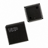
IC 80C51 MCU 512 RAM 44PLCC
Manufacturer
NXP Semiconductors
Series
87Cr
Datasheet
1.P87C51RC2FA512.pdf
(67 pages)
Specifications of P87C51RB2BA,512
Core Processor
8051
Core Size
8-Bit
Speed
33MHz
Connectivity
EBI/EMI, UART/USART
Peripherals
POR, PWM, WDT
Number Of I /o
32
Program Memory Size
16KB (16K x 8)
Program Memory Type
OTP
Ram Size
512 x 8
Voltage - Supply (vcc/vdd)
2.7 V ~ 5.5 V
Oscillator Type
Internal
Operating Temperature
0°C ~ 70°C
Package / Case
44-PLCC
Processor Series
P87C5x
Core
80C51
Data Bus Width
8 bit
Data Ram Size
512 B
Interface Type
UART
Maximum Clock Frequency
16 MHz
Number Of Programmable I/os
32
Number Of Timers
3
Operating Supply Voltage
2.7 V to 5.5 V
Maximum Operating Temperature
+ 70 C
Mounting Style
SMD/SMT
3rd Party Development Tools
PK51, CA51, A51, ULINK2
Minimum Operating Temperature
0 C
For Use With
OM10064 - EMULATOR 80C51 PDS51-MK2
Lead Free Status / RoHS Status
Lead free / RoHS Compliant
Eeprom Size
-
Data Converters
-
Lead Free Status / Rohs Status
Details
Other names
935271248512
P87C51RB2BA
P87C51RB2BA
P87C51RB2BA
P87C51RB2BA
Available stocks
Company
Part Number
Manufacturer
Quantity
Price
Company:

Part Number:
P87C51RB2BA,512
Manufacturer:
NXP Semiconductors
Quantity:
10 000


Philips Semiconductors
DC ELECTRICAL CHARACTERISTICS
T
NOTES:
1. Typical ratings are not guaranteed. The values listed are at room temperature, 5 V.
2. Capacitive loading on ports 0 and 2 may cause spurious noise to be superimposed on the V
3. Capacitive loading on ports 0 and 2 may cause the V
4. Pins of ports 1, 2 and 3 source a transition current when they are being externally driven from 1 to 0. The transition current reaches its
5. See Figures 43 through 46 for I
6. This value applies to T
7. Load capacitance for port 0, ALE, and PSEN = 100 pF, load capacitance for all other outputs = 80 pF.
8. Under steady state (non-transient) conditions, I
9. ALE is tested to V
10. Pin capacitance is characterized but not tested. Pin capacitance is less than 25 pF. Pin capacitance of ceramic package is less than 15 pF
11. To improve noise rejection a nominal 100 ns glitch rejection circuitry has been added to the RST pin, and a nominal 15 ns glitch rejection
2003 Jan 24
amb
SYMBOL PARAMETER
V
V
V
V
V
V
V
I
I
I
I
V
R
C
IL
TL
LI
CC
IL
IH
IH1
OL
OL1
OH
OH1
RAM
80C51 8-bit microcontroller family
with 512B/1KB RAM, low voltage (2.7 to 5.5 V), low power, high
speed (30/33 MHz)
RST
IO
to external bus capacitance discharging into the port 0 and port 2 pins when these pins make 1-to-0 transitions during bus operations. In the
worst cases (capacitive loading > 100 pF), the noise pulse on the ALE pin may exceed 0.8 V. In such cases, it may be desirable to qualify
ALE with a Schmitt Trigger, or use an address latch with a Schmitt Trigger STROBE input. I
single output sinks more than 5 mA and no more than two outputs exceed the test conditions.
address bits are stabilizing.
maximum value when V
12-clock mode characteristics:
If I
test conditions.
(except EA is 25 pF).
circuitry has been added to the INT0 and INT1 pins. Previous devices provided only an inherent 5 ns of glitch rejection.
= 0 C to +70 C or –40 C to +85 C; V
OL
Active mode (operating):
Active mode (reset):
Idle mode:
Maximum I
Maximum I
Maximum total I
exceeds the test condition, V
Input low voltage
Input high voltage (ports 0, 1, 2, 3, EA)
Input high voltage, XTAL1, RST
Output low voltage, ports 1, 2, 3
Output low voltage, port 0, ALE, PSEN
Output high voltage, ports 1, 2, 3
Output high voltage (port 0 in external bus
mode), ALE
Logical 0 input current, ports 1, 2, 3
Logical 1-to-0 transition current, ports 1, 2, 3
Input leakage current, port 0
Power supply current
Active mode (see Note 5)
Idle mode (see Note 5)
Power-down mode or clock stopped
(see Figure 46 for conditions)
RAM keep-alive voltage
Internal reset pull-down resistor
Pin capacitance
OL
OL
per port pin:
per 8-bit port:
OH1
OL
9
, except when ALE is off then V
amb
for all outputs:
, PSEN
IN
10
is approximately 2 V.
11
= 0 C to +70 C. For T
(except EA)
3
I
I
I
CC
CC
CC
CC
test conditions and Figure 41 for I
= 1.0 mA + 1.1 mA
= 7.0 mA + 0.6 mA
= 1.0 mA + 0.22 mA
OL
may exceed the related specification. Pins are not guaranteed to sink current greater than the listed
15 mA (*NOTE: This is 85 C specification.)
26 mA
71 mA
11
CC
8
8KB/16KB/32KB/64KB OTP
3
= 5 V 10%; V
OL
amb
7, 8
must be externally limited as follows:
= –40 C to +85 C, I
OH
OH
6
FREQ.[MHz]
on ALE and PSEN to momentarily fall below the V
is the voltage specification.
FREQ.[MHz]
TEST
CONDITIONS
4.5 V < V
V
V
V
V
V
V
0.45 < V
T
T
FREQ.[MHz]
amb
amb
CC
CC
CC
CC
IN
IN
SS
= 0.4 V
= 2.0 V; See note 4
= 4.5 V; I
= 4.5 V; I
= 4.5 V; I
= 4.5 V; I
= 0 C to 70 C
= –40 C to +85 C
= 0 V (30/33 MHz max. CPU clock)
IN
CC
45
< V
CC
< 5.5 V
OL
OL
OH
OH
vs. Frequency.
CC
TL
= 1.6 mA
= 3.2 mA
= –30 A
= –3.2 mA
– 0.3
= –750
2
2
.
LIMITS
MIN
–0.5
0.2 V
0.7 V
–
–
V
V
–1
–
–
1.2
40
–
CC
CC
P87C51RA2/RB2/RC2/RD2
OL
OL
– 0.7
– 0.7
CC
CC
s of ALE and ports 1 and 3. The noise is due
can exceed these conditions provided that no
+0.9
TYP
2
3
CC
1
–0.7 specification when the
MAX
0.2 V
V
V
0.4
0.4
–
–
–50
–650
30
50
225
15
10
CC
CC
+0.5
+0.5
CC
–0.1
Product data
UNIT
V
V
V
V
V
V
V
V
k
pF
A
A
A
A
A
Related parts for P87C51RB2BA,512
Image
Part Number
Description
Manufacturer
Datasheet
Request
R

Part Number:
Description:
80C51 8-bit microcontroller family
Manufacturer:
PHILIPS [NXP Semiconductors]
Datasheet:

Part Number:
Description:
IC 80C51 MCU 16K OTP 44-PLCC
Manufacturer:
NXP Semiconductors
Datasheet:

Part Number:
Description:
MCU 8-Bit 87C 80C51 CISC 16KB EPROM 3.3V/5V 44-Pin PLCC Tube
Manufacturer:
NXP Semiconductors
Datasheet:
Part Number:
Description:
NXP Semiconductors designed the LPC2420/2460 microcontroller around a 16-bit/32-bitARM7TDMI-S CPU core with real-time debug interfaces that include both JTAG andembedded trace
Manufacturer:
NXP Semiconductors
Datasheet:

Part Number:
Description:
NXP Semiconductors designed the LPC2458 microcontroller around a 16-bit/32-bitARM7TDMI-S CPU core with real-time debug interfaces that include both JTAG andembedded trace
Manufacturer:
NXP Semiconductors
Datasheet:
Part Number:
Description:
NXP Semiconductors designed the LPC2468 microcontroller around a 16-bit/32-bitARM7TDMI-S CPU core with real-time debug interfaces that include both JTAG andembedded trace
Manufacturer:
NXP Semiconductors
Datasheet:
Part Number:
Description:
NXP Semiconductors designed the LPC2470 microcontroller, powered by theARM7TDMI-S core, to be a highly integrated microcontroller for a wide range ofapplications that require advanced communications and high quality graphic displays
Manufacturer:
NXP Semiconductors
Datasheet:
Part Number:
Description:
NXP Semiconductors designed the LPC2478 microcontroller, powered by theARM7TDMI-S core, to be a highly integrated microcontroller for a wide range ofapplications that require advanced communications and high quality graphic displays
Manufacturer:
NXP Semiconductors
Datasheet:
Part Number:
Description:
The Philips Semiconductors XA (eXtended Architecture) family of 16-bit single-chip microcontrollers is powerful enough to easily handle the requirements of high performance embedded applications, yet inexpensive enough to compete in the market for hi
Manufacturer:
NXP Semiconductors
Datasheet:
Part Number:
Description:
The XA-S3 device is a member of Philips Semiconductors? XA(eXtended Architecture) family of high performance 16-bitsingle-chip microcontrollers
Manufacturer:
NXP Semiconductors
Datasheet:

Part Number:
Description:
The NXP BlueStreak LH75401/LH75411 family consists of two low-cost 16/32-bit System-on-Chip (SoC) devices
Manufacturer:
NXP Semiconductors
Datasheet:
Part Number:
Description:
The NXP LPC3130/3131 combine an 180 MHz ARM926EJ-S CPU core, high-speed USB2
Manufacturer:
NXP Semiconductors
Datasheet:
Part Number:
Description:
The NXP LPC3141 combine a 270 MHz ARM926EJ-S CPU core, High-speed USB 2
Manufacturer:
NXP Semiconductors
Part Number:
Description:
The NXP LPC3143 combine a 270 MHz ARM926EJ-S CPU core, High-speed USB 2
Manufacturer:
NXP Semiconductors