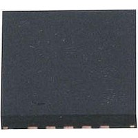
ATTINY25-15MZ Atmel, ATTINY25-15MZ Datasheet - Page 6

ATTINY25-15MZ
Manufacturer Part Number
ATTINY25-15MZ
Description
MCU AVR 2K FLASH 15MHZ 20-QFN
Manufacturer
Atmel
Series
AVR® ATtinyr
Datasheet
1.ATTINY25-15MZ.pdf
(196 pages)
Specifications of ATTINY25-15MZ
Package / Case
20-QFN
Voltage - Supply (vcc/vdd)
2.7 V ~ 5.5 V
Operating Temperature
-40°C ~ 125°C
Speed
16MHz
Number Of I /o
6
Eeprom Size
128 x 8
Core Processor
AVR
Program Memory Type
FLASH
Ram Size
128 x 8
Program Memory Size
2KB (2K x 8)
Data Converters
A/D 4x10b
Oscillator Type
Internal
Peripherals
Brown-out Detect/Reset, POR, PWM, WDT
Connectivity
USI
Core Size
8-Bit
Processor Series
ATTINY2x
Core
AVR8
Data Bus Width
8 bit
Data Ram Size
128 B
Interface Type
UART, SPI, USI
Maximum Clock Frequency
16 MHz
Number Of Programmable I/os
6
Number Of Timers
2
Maximum Operating Temperature
+ 85 C
Mounting Style
SMD/SMT
3rd Party Development Tools
EWAVR, EWAVR-BL
Development Tools By Supplier
ATAVRDRAGON, ATSTK500, ATSTK600, ATAVRISP2, ATAVRONEKIT
Minimum Operating Temperature
- 40 C
On-chip Adc
10 bit, 4 Channel
Data Rom Size
128 B
A/d Bit Size
10 bit
A/d Channels Available
4
Height
0.75 mm
Length
4 mm
Supply Voltage (max)
5.5 V
Supply Voltage (min)
2.7 V
Width
4 mm
Lead Free Status / RoHS Status
Lead free / RoHS Compliant
- Current page: 6 of 196
- Download datasheet (4Mb)
4.2
6
Architectural Overview
ATtiny25/45/85
Figure 4-1.
In order to maximize performance and parallelism, the AVR uses a Harvard architecture – with
separate memories and buses for program and data. Instructions in the Program memory are
executed with a single level pipelining. While one instruction is being executed, the next instruc-
tion is pre-fetched from the Program memory. This concept enables instructions to be executed
in every clock cycle. The Program memory is In-System Reprogrammable Flash memory.
The fast-access Register File contains 32 x 8-bit general purpose working registers with a single
clock cycle access time. This allows single-cycle Arithmetic Logic Unit (ALU) operation. In a typ-
ical ALU operation, two operands are output from the Register File, the operation is executed,
and the result is stored back in the Register File – in one clock cycle.
Six of the 32 registers can be used as three 16-bit indirect address register pointers for Data
Space addressing – enabling efficient address calculations. One of the these address pointers
can also be used as an address pointer for look up tables in Flash Program memory. These
added function registers are the 16-bit X-, Y-, and Z-register, described later in this section.
Control Lines
Instruction
Instruction
Program
Memory
Block Diagram of the AVR Architecture
Register
Decoder
Flash
Program
Counter
and Control
EEPROM
Registrers
I/O Lines
Purpose
General
SRAM
Data Bus 8-bit
Status
32 x 8
Data
ALU
I/O Module 2
Comparator
I/O Module1
I/O Module n
Watchdog
Interrupt
Timer
Analog
Unit
7598H–AVR–07/09
Related parts for ATTINY25-15MZ
Image
Part Number
Description
Manufacturer
Datasheet
Request
R

Part Number:
Description:
Manufacturer:
Atmel Corporation
Datasheet:

Part Number:
Description:
Manufacturer:
Atmel Corporation
Datasheet:

Part Number:
Description:
IC MCU AVR 2K FLASH 20MHZ 20-QFN
Manufacturer:
Atmel
Datasheet:

Part Number:
Description:
IC AVR MCU 2K 20MHZ 8-DIP
Manufacturer:
Atmel
Datasheet:

Part Number:
Description:
IC AVR MCU 2K 20MHZ 8-SOIC
Manufacturer:
Atmel
Datasheet:

Part Number:
Description:
8-bit Microcontrollers - MCU AVR 16KB FL 512B EE 1KB SRAM 10 MHZ GRN
Manufacturer:
Atmel

Part Number:
Description:
8-bit Microcontrollers - MCU AVR 16KB FL 512B EE 1KB SRAM 10 MHZ GRN
Manufacturer:
Atmel

Part Number:
Description:
MCU AVR 2K ISP FLASH 2.7V 8-SOIC
Manufacturer:
Atmel
Datasheet:

Part Number:
Description:
MCU AVR 2KB FLASH 20MHZ 8SOIC
Manufacturer:
Atmel
Datasheet:

Part Number:
Description:
IC MCU AVR 2KB FLASH 20MHZ 8SOIC
Manufacturer:
Atmel
Datasheet:

Part Number:
Description:
IC MCU AVR 2KB FLASH 20MHZ 8SOIC
Manufacturer:
Atmel
Datasheet:

Part Number:
Description:
MCU AVR 2KB FLASH 20MHZ 8SOIC
Manufacturer:
Atmel
Datasheet:

Part Number:
Description:
MCU AVR 2KB FLASH 20MHZ 8SOIC
Manufacturer:
Atmel
Datasheet:

Part Number:
Description:
MCU AVR 2KB FLASH 20MHZ 20QFN
Manufacturer:
Atmel
Datasheet:


