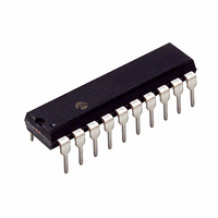
PIC16C770/P Microchip Technology, PIC16C770/P Datasheet - Page 37

PIC16C770/P
Manufacturer Part Number
PIC16C770/P
Description
IC MCU CMOS A/D 2K 20MHZ 20-DIP
Manufacturer
Microchip Technology
Series
PIC® 16Cr
Datasheets
1.PIC16C770-ISO.pdf
(220 pages)
2.PIC16C770-ISO.pdf
(6 pages)
3.PIC16C770-ISO.pdf
(8 pages)
Specifications of PIC16C770/P
Program Memory Type
OTP
Program Memory Size
3.5KB (2K x 14)
Package / Case
20-DIP (0.300", 7.62mm)
Core Processor
PIC
Core Size
8-Bit
Speed
20MHz
Connectivity
I²C, SPI
Peripherals
Brown-out Detect/Reset, POR, PWM, WDT
Number Of I /o
15
Ram Size
256 x 8
Voltage - Supply (vcc/vdd)
4 V ~ 5.5 V
Data Converters
A/D 6x12b
Oscillator Type
Internal
Operating Temperature
0°C ~ 70°C
Processor Series
PIC16C
Core
PIC
Data Bus Width
8 bit
Data Ram Size
256 B
Interface Type
I2C/SPI/SSP
Maximum Clock Frequency
20 MHz
Number Of Programmable I/os
16
Number Of Timers
3
Operating Supply Voltage
2.5 V to 5.5 V
Maximum Operating Temperature
+ 70 C
Mounting Style
Through Hole
3rd Party Development Tools
52715-96, 52716-328, 52717-734
Development Tools By Supplier
ICE2000
Minimum Operating Temperature
0 C
On-chip Adc
6-ch x 12-bit
Lead Free Status / RoHS Status
Lead free / RoHS Compliant
For Use With
DVA16XP200 - ADAPTER ICE 20DIP/SOIC/SSOPAC164028 - MODULE SKT PROMATEII 20SOIC/DIP
Eeprom Size
-
Lead Free Status / Rohs Status
Lead free / RoHS Compliant
- Current page: 37 of 220
- Download datasheet (4Mb)
The RB0 pin is multiplexed with the A/D converter ana-
log input 4 and the external interrupt input (RB0/AN4/
INT). When the pin is used as analog input, the ANSEL
register must have the proper value to select the RB0
pin as Analog mode.
FIGURE 3-7:
2002 Microchip Technology Inc.
To INT input or MSSP module
To A/D Converter
Data Bus
WR
WPUB
WR
PORT
WR
TRIS
RD
TRIS
WR
ANSEL
WR
IOCB
RD
PORT
BLOCK DIAGRAM OF RB0/AN4/INT, RB1/AN5/SS PIN
PORTB Reg
Analog Select
WPUB Reg
TRIS Reg
IOCB Reg
D
D
CK
CK
D
D
D
CK
CK
CK
Q
Q
Q
Q
Q
Q
Q
Q
Q
Q
Set
RBIF
RBPU
From
RB<7:0> pins
Q
EN
EN
D
The RB1 pin is multiplexed with the A/D converter ana-
log input 5 and the MSSP module slave select input
(RB1/AN5/SS). When the pin is used as analog input,
the ANSEL register must have the proper value to
select the RB1 pin as Analog mode.
Note:
V
V
P
N
PIC16C717/770/771
SS
DD
Upon RESET, the ANSEL register config-
ures the RB1 and RB0 pins as analog inputs.
Both RB1 and RB0 pins will read as ’1’.
Q
Q
EN
EN
D
D
TTL
V
P
DD
weak
pull-up
Schmitt
Trigger
Q1
Q3
DS41120B-page 35
V
DD
V
SS
Related parts for PIC16C770/P
Image
Part Number
Description
Manufacturer
Datasheet
Request
R

Part Number:
Description:
IC, 8BIT MCU, PIC16C, 40MHZ, DIP-18
Manufacturer:
Microchip Technology
Datasheet:

Part Number:
Description:
IC, 8BIT MCU, PIC16C, 4MHZ, DIP-28
Manufacturer:
Microchip Technology
Datasheet:

Part Number:
Description:
IC, 8BIT MCU, PIC16C, 4MHZ, DIP-28
Manufacturer:
Microchip Technology
Datasheet:

Part Number:
Description:
IC, 8BIT MCU, PIC16C, 4MHZ, DIP-40
Manufacturer:
Microchip Technology
Datasheet:

Part Number:
Description:
SURFACE MOUNT POWER INDUCTORS
Manufacturer:
RCD [RCD COMPONENTS INC.]
Datasheet:

Part Number:
Description:
Manufacturer:
Microchip Technology Inc.
Datasheet:

Part Number:
Description:
Manufacturer:
Microchip Technology Inc.
Datasheet:

Part Number:
Description:
Manufacturer:
Microchip Technology Inc.
Datasheet:

Part Number:
Description:
Manufacturer:
Microchip Technology Inc.
Datasheet:

Part Number:
Description:
Manufacturer:
Microchip Technology Inc.
Datasheet:

Part Number:
Description:
Manufacturer:
Microchip Technology Inc.
Datasheet:


