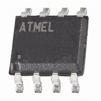
ATTINY13A-SU Atmel, ATTINY13A-SU Datasheet - Page 31

ATTINY13A-SU
Manufacturer Part Number
ATTINY13A-SU
Description
IC MCU AVR 1K FLASH 20MHZ 8SOIC
Manufacturer
Atmel
Series
AVR® ATtinyr
Specifications of ATTINY13A-SU
Core Processor
AVR
Core Size
8-Bit
Speed
20MHz
Peripherals
Brown-out Detect/Reset, POR, PWM, WDT
Number Of I /o
6
Program Memory Size
1KB (512 x 16)
Program Memory Type
FLASH
Eeprom Size
64 x 8
Ram Size
64 x 8
Voltage - Supply (vcc/vdd)
1.8 V ~ 5.5 V
Data Converters
A/D 4x10b
Oscillator Type
Internal
Operating Temperature
-40°C ~ 85°C
Package / Case
8-SOIC (5.3mm Width), 8-SOP, 8-SOEIAJ
Cpu Family
ATtiny
Device Core
AVR
Device Core Size
8b
Frequency (max)
20MHz
Interface Type
SPI
Total Internal Ram Size
64Byte
# I/os (max)
6
Number Of Timers - General Purpose
1
Operating Supply Voltage (typ)
2.5/3.3/5V
Operating Supply Voltage (max)
5.5V
Operating Supply Voltage (min)
1.8V
On-chip Adc
4-chx10-bit
Instruction Set Architecture
RISC
Operating Temp Range
-40C to 85C
Operating Temperature Classification
Industrial
Mounting
Surface Mount
Pin Count
8
Package Type
SOIC EIAJ
Processor Series
ATTINY1x
Core
AVR8
Data Bus Width
8 bit
Data Ram Size
64 B
Maximum Clock Frequency
20 MHz
Number Of Programmable I/os
6
Number Of Timers
1
Maximum Operating Temperature
+ 85 C
Mounting Style
SMD/SMT
3rd Party Development Tools
EWAVR, EWAVR-BL
Development Tools By Supplier
ATAVRDRAGON, ATSTK500, ATSTK600, ATAVRISP2, ATAVRONEKIT, ATAKSTK511
Minimum Operating Temperature
- 40 C
Package
8SOIC EIAJ
Family Name
ATtiny
Maximum Speed
20 MHz
Operating Supply Voltage
2.5|3.3|5 V
For Use With
ATSTK600-DIP40 - STK600 SOCKET/ADAPTER 40-PDIP770-1007 - ISP 4PORT ATMEL AVR MCU SPI/JTAG770-1004 - ISP 4PORT FOR ATMEL AVR MCU SPIATAVRDRAGON - KIT DRAGON 32KB FLASH MEM AVRATAVRISP2 - PROGRAMMER AVR IN SYSTEMATJTAGICE2 - AVR ON-CHIP D-BUG SYSTEM
Lead Free Status / RoHS Status
Lead free / RoHS Compliant
Connectivity
-
Lead Free Status / Rohs Status
Compliant
Available stocks
Company
Part Number
Manufacturer
Quantity
Price
Company:
Part Number:
ATTINY13A-SU
Manufacturer:
TI
Quantity:
21 550
Part Number:
ATTINY13A-SU
Manufacturer:
ATMEL/爱特梅尔
Quantity:
20 000
7.1.2
7.1.3
7.2
7.3
8126E–AVR–07/10
Software BOD Disable
Power Reduction Register
ADC Noise Reduction Mode
Power-down Mode
Control and Status Register – ACSR. This will reduce power consumption in Idle mode. If the
ADC is enabled, a conversion starts automatically when this mode is entered.
When the SM[1:0] bits are written to 01, the SLEEP instruction makes the MCU enter ADC
Noise Reduction mode, stopping the CPU but allowing the ADC, the external interrupts, and the
Watchdog to continue operating (if enabled). This sleep mode halts clk
while allowing the other clocks to run.
This improves the noise environment for the ADC, enabling higher resolution measurements. If
the ADC is enabled, a conversion starts automatically when this mode is entered. Apart form the
ADC Conversion Complete interrupt, only an External Reset, a Watchdog Reset, a Brown-out
Reset, an SPM/EEPROM ready interrupt, an external level interrupt on INT0 or a pin change
interrupt can wake up the MCU from ADC Noise Reduction mode.
When the SM[1:0] bits are written to 10, the SLEEP instruction makes the MCU enter Power-
down mode. In this mode, the Oscillator is stopped, while the external interrupts, and the Watch-
dog continue operating (if enabled). Only an External Reset, a Watchdog Reset, a Brown-out
Reset, an external level interrupt on INT0, or a pin change interrupt can wake up the MCU. This
sleep mode halts all generated clocks, allowing operation of asynchronous modules only.
When the Brown-out Detector (BOD) is enabled by BODLEVEL fuses (see
104), the BOD is actively monitoring the supply voltage during a sleep period. It is possible to
save power by disabling the BOD by software in Power-Down sleep mode. The sleep mode
power consumption will then be at the same level as when BOD is globally disabled by fuses.
If BOD is disabled by software, the BOD function is turned off immediately after entering the
sleep mode. Upon wake-up from sleep, BOD is automatically enabled again. This ensures safe
operation in case the V
When the BOD has been disabled, the wake-up time from sleep mode will be approximately
60µs to ensure that the BOD is working correctly before the MCU continues executing code.
BOD disable is controlled by the BODS (BOD Sleep) bit of BOD Control Register, see
– Brown-Out Detector Control Register” on page
Power-Down and Stand-By, while writing a zero keeps the BOD active. The default setting is
zero, i.e. BOD active.
Writing to the BODS bit is controlled by a timed sequence and an enable bit, see
Brown-Out Detector Control Register” on page
The Power Reduction Register (see
method to reduce power consumption by stopping the clock to individual peripherals. The cur-
rent state of the peripheral is frozen and the I/O registers can not be read or written. When
stopping the clock resources used by the peripheral will remain occupied, hence the peripheral
should in most cases be disabled before stopping the clock. Waking up a module (by clearing
the bit in PRR) puts the module in the same state as before shutdown.
CC
level has dropped during the sleep period.
“PRR – Power Reduction Register” on page
33.
33. Writing this bit to one turns off BOD in
I/O
, clk
Table 17-3 on page
CPU
, and clk
34) provides a
“BODCR –
“BODCR
FLASH
31
,


