M30879FKBGP#U5 Renesas Electronics America, M30879FKBGP#U5 Datasheet - Page 122
M30879FKBGP#U5
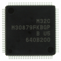
Manufacturer Part Number
M30879FKBGP#U5
Description
IC M32C/87 MCU FLASH 100LQFP
Manufacturer
Renesas Electronics America
Series
M16C™ M32C/80r
Datasheet
1.M3087BFLGPU3.pdf
(629 pages)
Specifications of M30879FKBGP#U5
Core Processor
M32C/80
Core Size
16/32-Bit
Speed
32MHz
Connectivity
EBI/EMI, I²C, IEBus, IrDA, SIO, UART/USART
Peripherals
DMA, POR, PWM, WDT
Number Of I /o
85
Program Memory Size
768KB (768K x 8)
Program Memory Type
FLASH
Ram Size
48K x 8
Voltage - Supply (vcc/vdd)
3 V ~ 5.5 V
Data Converters
A/D 26x10b; D/A 2x8b
Oscillator Type
Internal
Operating Temperature
-20°C ~ 85°C
Package / Case
100-LQFP
For Use With
R0K330879S001BE - KIT DEV RSK M32C/87R0K330879S000BE - KIT DEV RSK M32C/87
Lead Free Status / RoHS Status
Lead free / RoHS Compliant
Eeprom Size
-
Available stocks
Company
Part Number
Manufacturer
Quantity
Price

Part Number:
M30879FKBGP#U5M30879FKBGP#U3
Manufacturer:
Renesas Electronics America
Quantity:
10 000


M32C/87 Group (M32C/87, M32C/87A, M32C/87B)
REJ09B0180-0151 Rev.1.51 Jul 31, 2008
Page 98 of 587
Table 9.6
NOTES:
9.5.2
Main clock
PLL clock
Sub clock
On-chip
oscillator clock
9.5.2.1
9.5.2.2
CPU Clock
1. The CM21 bit in the CM2 register has both the oscillation control and selector functions.
2. Refer to 23.2 CAN Clock and CPU Clock for details.
Source
In wait mode, the CPU and watchdog timer stop operating. If the PM22 bit in the PM2 register is set to 1 (on-
chip oscillator clock as watchdog timer count source), the watchdog timer continues operating. Since the main
clock, sub clock, and on-chip oscillator clock continue running, peripheral functions using these clocks as their
clock source also continue to operate.
If the CM02 bit in the CM0 register is set to 1 (peripheral clocks stop in wait mode), fAD, f1, f8, and f32 stop in
wait mode. f2n, which uses the clock selected by the CM21 bit in the CM2 register as its clock source, also
stops in wait mode. Power consumption can be reduced by stopping these peripheral clocks. f2n, which uses the
XIN clock (fXIND) or on-chip oscillator clock as its clock source, and fC32 do not stop even in wait mode.
To enter wait mode with the CM02 bit in the CM0 register set to 1, set bits MCD4 to MCD0 in the MCD
register for the CPU clock frequency to be 10 MHz or lower after dividing the main clock.
Figure 9.14 shows a procedure to enter wait mode.
Wait Mode
Operation Mode Setting
Peripheral Function Clock Stop Function
Entering Wait Mode
Main clock mode
Main clock direct
mode
PLL mode
Low-speed mode
Low power
consumption mode
On-chip oscillator mode
On-chip oscillator low-
power consumption
mode
Operating Mode
(2)
CM05
CM0 Register
0
0
0
0
1
0
1
Oscillation Control
CM04
0 or 1
0 or 1
0 or 1
0 or 1
0 or 1
1
1
Register
PLC07
0 or 1
0 or 1
0 or 1
0 or 1
PLC0
1
0
0
Register
CM21
CM2
0
0
0
0
0
1
1
(1)
Register
CM17
CM1
9. Clock Generation Circuits
0
0
1
0
0
0
0
Register
Selector
CM07
CM0
0
0
0
1
1
0
0
Register
PM24
PM2
0
1
0
0
0
0
0
Related parts for M30879FKBGP#U5
Image
Part Number
Description
Manufacturer
Datasheet
Request
R

Part Number:
Description:
KIT STARTER FOR M16C/29
Manufacturer:
Renesas Electronics America
Datasheet:

Part Number:
Description:
KIT STARTER FOR R8C/2D
Manufacturer:
Renesas Electronics America
Datasheet:

Part Number:
Description:
R0K33062P STARTER KIT
Manufacturer:
Renesas Electronics America
Datasheet:

Part Number:
Description:
KIT STARTER FOR R8C/23 E8A
Manufacturer:
Renesas Electronics America
Datasheet:

Part Number:
Description:
KIT STARTER FOR R8C/25
Manufacturer:
Renesas Electronics America
Datasheet:

Part Number:
Description:
KIT STARTER H8S2456 SHARPE DSPLY
Manufacturer:
Renesas Electronics America
Datasheet:

Part Number:
Description:
KIT STARTER FOR R8C38C
Manufacturer:
Renesas Electronics America
Datasheet:

Part Number:
Description:
KIT STARTER FOR R8C35C
Manufacturer:
Renesas Electronics America
Datasheet:

Part Number:
Description:
KIT STARTER FOR R8CL3AC+LCD APPS
Manufacturer:
Renesas Electronics America
Datasheet:
Part Number:
Description:
KIT STARTER FOR RX610
Manufacturer:
Renesas Electronics America
Datasheet:

Part Number:
Description:
KIT STARTER FOR R32C/118
Manufacturer:
Renesas Electronics America
Datasheet:

Part Number:
Description:
KIT DEV RSK-R8C/26-29
Manufacturer:
Renesas Electronics America
Datasheet:

Part Number:
Description:
KIT STARTER FOR SH7124
Manufacturer:
Renesas Electronics America
Datasheet:

Part Number:
Description:
KIT STARTER FOR H8SX/1622
Manufacturer:
Renesas Electronics America
Datasheet:

Part Number:
Description:
KIT DEV FOR SH7203
Manufacturer:
Renesas Electronics America
Datasheet: