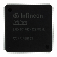
SAK-TC1762-128F80HL AC Infineon Technologies, SAK-TC1762-128F80HL AC Datasheet - Page 28

SAK-TC1762-128F80HL AC
Manufacturer Part Number
SAK-TC1762-128F80HL AC
Description
IC MCU 32BIT FLASH PG-LQFP-176
Manufacturer
Infineon Technologies
Series
TC17xxr
Datasheet
1.SAK-TC1762-128F80HL_AC.pdf
(114 pages)
Specifications of SAK-TC1762-128F80HL AC
Core Processor
TriCore
Core Size
32-Bit
Speed
80MHz
Connectivity
ASC, CAN, MLI, MSC, SSC
Peripherals
DMA, POR, WDT
Number Of I /o
81
Program Memory Size
1MB (1M x 8)
Program Memory Type
FLASH
Ram Size
52K x 8
Voltage - Supply (vcc/vdd)
1.42 V ~ 1.58 V
Data Converters
A/D 2x10b; A/D 32x8b,10b,12b
Oscillator Type
External
Operating Temperature
-40°C ~ 125°C
Package / Case
176-LFQFP
Packages
PG-LQFP-176
Max Clock Frequency
80.0 MHz
Sram (incl. Cache)
52.0 KByte
Can Nodes
2
A / D Input Lines (incl. Fadc)
36
Program Memory
1.0 MB
For Use With
B158-H8539-G2-X-7600IN - KIT STARTER TC176X SERIES
Lead Free Status / RoHS Status
Lead free / RoHS Compliant
Eeprom Size
-
Other names
KT1762128F80HLACXT
SAK-TC1762-128F80HLACINTR
SP000318061
SAK-TC1762-128F80HLACINTR
SP000318061
Preliminary
3
Chapter 3
3.1
The TC1762 has two independent on-chip buses (see also TC1762 block diagram on
Page
•
•
The LMB Bus connects the CPU local resources for data and instruction fetch. The Local
Memory Bus interconnects the memory units and functional units, such as CPU and
PMU. The main target of the LMB bus is to support devices with fast response times,
optimized for speed. This allows the DMI and PMI fast access to local memory and
reduces load on the FPI bus. The Tricore system itself is located on LMB bus.
The Local Memory Bus is a synchronous, pipelined, split bus with variable block size
transfer support. It supports 8-, 16-, 32- and 64-bit single transactions and variable
length 64-bit block transfers.
The SPB Bus is accessible to the CPU via the LMB Bus bridge. The System Peripheral
Bus (SPB Bus) in TC1762 is an on-chip FPI Bus. The FPI Bus interconnects the
functional units of the TC1762, such as the DMA and on-chip peripheral components.
The FPI Bus is designed to be quick to be acquired by on-chip functional units, and quick
to transfer data. The low setup overhead of the FPI Bus access protocol guarantees fast
FPI Bus acquisition, which is required for time-critical applications.The FPI Bus is
designed to sustain high transfer rates. For example, a peak transfer rate of up to 320
Mbyte/s can be achieved with a 80 MHz bus clock and 32-bit data bus. With a 66 MHz
bus clock, the peak transfer rate is up to 264 Mbytes/s. Multiple data transfers per bus
arbitration cycle allow the FPI Bus to operate at close to its peak bandwidth.
Both the LMB Bus and the SPB Bus runs at full CPU speed. The maximum CPU speed
is 66 or 80 MHz depending on the derivative.
Additionally, two simplified bus interfaces are connected to and controlled by the DMA
Controller:
•
•
Data Sheet
Local Memory Bus (LMB)
System Peripheral Bus (SPB)
DMA Bus
SMIF Interface
2-6):
provides an overview of the TC1762 functional description.
Functional Description
System Architecture and On-Chip Bus Systems
24
Functional Description
V1.0, 2008-04
TC1762


