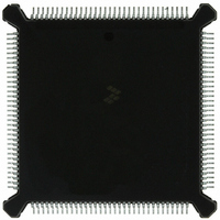
MC68332GCEH16 Freescale Semiconductor, MC68332GCEH16 Datasheet - Page 32

MC68332GCEH16
Manufacturer Part Number
MC68332GCEH16
Description
IC MCU 32BIT 16MHZ 132-PQFP
Manufacturer
Freescale Semiconductor
Series
M683xxr
Specifications of MC68332GCEH16
Core Processor
CPU32
Core Size
32-Bit
Speed
16MHz
Connectivity
EBI/EMI, SCI, SPI, UART/USART
Peripherals
POR, PWM, WDT
Number Of I /o
15
Program Memory Type
ROMless
Ram Size
2K x 8
Voltage - Supply (vcc/vdd)
4.5 V ~ 5.5 V
Oscillator Type
Internal
Operating Temperature
-40°C ~ 85°C
Package / Case
132-QFP
Cpu Family
68K/M683xx
Device Core
ColdFire
Device Core Size
32b
Frequency (max)
16MHz
Interface Type
QSPI/SCI/UART
Program Memory Size
Not Required
Total Internal Ram Size
2KB
# I/os (max)
15
Number Of Timers - General Purpose
16
Operating Supply Voltage (typ)
5V
Operating Supply Voltage (max)
5.5V
Operating Supply Voltage (min)
4.5V
Instruction Set Architecture
RISC
Operating Temp Range
-40C to 85C
Operating Temperature Classification
Industrial
Mounting
Surface Mount
Pin Count
132
Package Type
PQFP
Controller Family/series
68K
No. Of I/o's
15
Ram Memory Size
2KB
Cpu Speed
16MHz
No. Of Timers
16
Embedded Interface Type
QSPI, SCI, UART
Digital Ic Case Style
PQFP
Rohs Compliant
Yes
Processor Series
M683xx
Core
CPU32
Data Bus Width
32 bit
Data Ram Size
2 KB
Maximum Clock Frequency
16 MHz
Number Of Programmable I/os
15
Number Of Timers
16
Maximum Operating Temperature
+ 85 C
Mounting Style
SMD/SMT
Minimum Operating Temperature
- 40 C
Lead Free Status / RoHS Status
Lead free / RoHS Compliant
Eeprom Size
-
Program Memory Size
-
Data Converters
-
Lead Free Status / Rohs Status
Compliant
Available stocks
Company
Part Number
Manufacturer
Quantity
Price
Company:
Part Number:
MC68332GCEH16
Manufacturer:
Freescale Semiconductor
Quantity:
10 000
CSPAR1 —Chip Select Pin Assignment Register 1
32
MOTOROLA
RESET:
15
0
0
CSPAR1 contains five 2-bit fields that determine the functions of corresponding chip-select pins.
CSPAR1[15:10] are not used. These bits always read zero; writes have no effect.
At reset, either the alternate function (01) or chip-select function (11) can be encoded. DATA pins are
driven to logic level one by a weak interval pull-up during reset. Encoding is for chip-select function un-
less a data line is held low during reset. Note that bus loading can overcome the weak pull-up and hold
pins low during reset. The following table shows the hierarchical selection method that determines the
reset functions of pins controlled by CSPAR1.
When a pin is programmed for discrete output or alternate function, internal chip-select logic still func-
tions and can be used to generate DSACK or AVEC internally on an address match.
Port size is determined when a pin is assigned as a chip select. When a pin is assigned to an 8-bit port,
the chip select is asserted at all addresses within the block range. If a pin is assigned to a 16-bit port,
the upper/lower byte field of the option register selects the byte with which the chip select is associated.
DATA7
A pin programmed as a discrete output drives an external signal to the value specified in the port C
pin data register (PORTC), with the following exceptions:
1
1
1
1
1
0
CSPAR0 Field
14
0
0
CSPA1[4]
CSPA1[3]
CSPA1[2]
CSPA1[1]
CSPA1[0]
1. No discrete output function is available on pins BR, BG, or BGACK.
2. ADDR23 provides E-clock output rather than a discrete output signal.
DATA6
13
Data Bus Pins at Reset
0
0
X
1
1
1
1
0
12
0
0
DATA5
X
X
Freescale Semiconductor, Inc.
1
1
1
0
11
For More Information On This Product,
0
0
Table 15 Reset Pin Function of CS[10:6]
Chip Select Signal
Table 14 CSPAR1 Pin Assignments
DATA4
10
0
0
1
1
0
X
X
X
CS10
CS9
CS8
CS7
CS6
Go to: www.freescale.com
DATA7
9
CSPA1[4]
DATA3
1
0
X
X
X
X
8
1
ADDR23
ADDR23 ADDR22 ADDR21 ADDR20 ADDR19
DATA
CS10/
CS10
CS10
CS10
CS10
CS10
[7:6]
7
CSPA1[3]
Alternate Signal
Chip-Select/Address Bus Pin Function
ADDR23
ADDR22
ADDR21
ADDR20
ADDR19
6
1
ADDR22
ADDR22 ADDR21 ADDR20 ADDR19
CS9/
CS9
CS9
CS9
CS9
DATA
[7:5]
5
CSPA1[2]
ADDR21
ADDR21 ADDR20 ADDR19
CS8/
CS8
CS8
CS8
4
1
DATA
[7:4]
Discrete Output
3
CSPA1[1]
ADDR20
ADDR20 ADDR19
CS7/
CS7
CS7
ECLK
PC6
PC5
PC4
PC3
2
1
MC68332TS/D
ADDR19
ADDR19
DATA
[7:3]
CS6/
CS6
$YFFA46
1
MC68332
CSPA1[0]
0
1


