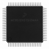
MC9S12XDT512MAA Freescale Semiconductor, MC9S12XDT512MAA Datasheet - Page 120

MC9S12XDT512MAA
Manufacturer Part Number
MC9S12XDT512MAA
Description
IC MCU 512K FLASH 80-QFP
Manufacturer
Freescale Semiconductor
Series
HCS12r
Datasheet
1.MC9S12XD64CAA.pdf
(1348 pages)
Specifications of MC9S12XDT512MAA
Core Processor
HCS12X
Core Size
16-Bit
Speed
80MHz
Connectivity
CAN, EBI/EMI, I²C, IrDA, LIN, SCI, SPI
Peripherals
LVD, POR, PWM, WDT
Number Of I /o
59
Program Memory Size
512KB (512K x 8)
Program Memory Type
FLASH
Eeprom Size
4K x 8
Ram Size
20K x 8
Voltage - Supply (vcc/vdd)
2.35 V ~ 5.5 V
Data Converters
A/D 8x10b
Oscillator Type
External
Operating Temperature
-40°C ~ 125°C
Package / Case
80-QFP
Processor Series
S12XD
Core
HCS12
Data Bus Width
16 bit
Data Ram Size
32 KB
Interface Type
CAN/I2C/SCI/SPI
Maximum Clock Frequency
40 MHz
Number Of Programmable I/os
59
Number Of Timers
12
Operating Supply Voltage
0 V to 5.5 V
Maximum Operating Temperature
+ 125 C
Mounting Style
SMD/SMT
3rd Party Development Tools
EWHCS12
Development Tools By Supplier
EVB9S12XDP512E
Minimum Operating Temperature
- 40 C
On-chip Adc
8-ch x 10-bit
Package
80PQFP
Family Name
HCS12
Maximum Speed
40 MHz
Lead Free Status / RoHS Status
Lead free / RoHS Compliant
Available stocks
Company
Part Number
Manufacturer
Quantity
Price
Company:
Part Number:
MC9S12XDT512MAA
Manufacturer:
Freescale Semiconductor
Quantity:
10 000
- Current page: 120 of 1348
- Download datasheet (8Mb)
Chapter 3 Pierce Oscillator (S12XOSCLCPV1)
3.1.3
Figure 3-1
3.2
This section lists and describes the signals that connect off chip
3.2.1
Theses pins provides operating voltage (V
allows the supply voltage to the XOSC to be independently bypassed.
3.2.2
These pins provide the interface for either a crystal or a CMOS compatible clock to control the internal
clock generator circuitry. EXTAL is the external clock input or the input to the crystal oscillator amplifier.
XTAL is the output of the crystal oscillator amplifier. The MCU internal system clock is derived from the
120
External Signal Description
shows a block diagram of the XOSC.
Block Diagram
V
EXTAL and XTAL — Input and Output Pins
DDPLL
and V
Detector
Peak
EXTAL
SSPLL
MC9S12XDP512 Data Sheet, Rev. 2.21
Figure 3-1. XOSC Block Diagram
— Operating and Ground Voltage Pins
Gain Control
DDPLL
Monitor
Clock
) and ground (V
Rf
V
DDPLL
Monitor_Failure
= 2.5 V
OSCCLK
SSPLL
XTAL
) for the XOSC circuitry. This
Freescale Semiconductor
Related parts for MC9S12XDT512MAA
Image
Part Number
Description
Manufacturer
Datasheet
Request
R

Part Number:
Description:
16-BIT MICROPROCESSOR FAMILY
Manufacturer:
FREESCALE [Freescale Semiconductor, Inc]
Datasheet:
Part Number:
Description:
Manufacturer:
Freescale Semiconductor, Inc
Datasheet:
Part Number:
Description:
Manufacturer:
Freescale Semiconductor, Inc
Datasheet:
Part Number:
Description:
Manufacturer:
Freescale Semiconductor, Inc
Datasheet:
Part Number:
Description:
Manufacturer:
Freescale Semiconductor, Inc
Datasheet:
Part Number:
Description:
Manufacturer:
Freescale Semiconductor, Inc
Datasheet:
Part Number:
Description:
Manufacturer:
Freescale Semiconductor, Inc
Datasheet:
Part Number:
Description:
Manufacturer:
Freescale Semiconductor, Inc
Datasheet:
Part Number:
Description:
Manufacturer:
Freescale Semiconductor, Inc
Datasheet:
Part Number:
Description:
Manufacturer:
Freescale Semiconductor, Inc
Datasheet:
Part Number:
Description:
Manufacturer:
Freescale Semiconductor, Inc
Datasheet:
Part Number:
Description:
Manufacturer:
Freescale Semiconductor, Inc
Datasheet:
Part Number:
Description:
Manufacturer:
Freescale Semiconductor, Inc
Datasheet:
Part Number:
Description:
Manufacturer:
Freescale Semiconductor, Inc
Datasheet:
Part Number:
Description:
Manufacturer:
Freescale Semiconductor, Inc
Datasheet:


