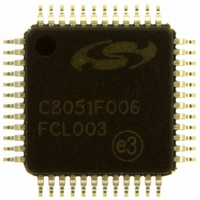
C8051F006-GQ Silicon Laboratories Inc, C8051F006-GQ Datasheet - Page 155

C8051F006-GQ
Manufacturer Part Number
C8051F006-GQ
Description
IC 8051 MCU 32K FLASH 48TQFP
Manufacturer
Silicon Laboratories Inc
Series
C8051F00xr
Specifications of C8051F006-GQ
Program Memory Type
FLASH
Program Memory Size
32KB (32K x 8)
Package / Case
48-TQFP, 48-VQFP
Core Processor
8051
Core Size
8-Bit
Speed
25MHz
Connectivity
SMBus (2-Wire/I²C), SPI, UART/USART
Peripherals
Brown-out Detect/Reset, POR, PWM, Temp Sensor, WDT
Number Of I /o
16
Ram Size
2.25K x 8
Voltage - Supply (vcc/vdd)
2.7 V ~ 3.6 V
Data Converters
A/D 8x12b, D/A 2x12b
Oscillator Type
Internal
Operating Temperature
-40°C ~ 85°C
Processor Series
C8051F0x
Core
8051
Data Bus Width
8 bit
Data Ram Size
2.25 KB
Interface Type
I2C/SMBus/SPI/UART
Maximum Clock Frequency
25 MHz
Number Of Programmable I/os
16
Number Of Timers
4
Operating Supply Voltage
2.7 V to 3.6 V
Maximum Operating Temperature
+ 85 C
Mounting Style
SMD/SMT
3rd Party Development Tools
PK51, CA51, A51, ULINK2
Development Tools By Supplier
C8051F005DK
Minimum Operating Temperature
- 40 C
On-chip Adc
8-ch x 12-bit
On-chip Dac
2-ch x 12-bit
Lead Free Status / RoHS Status
Lead free / RoHS Compliant
For Use With
336-1188 - DEV KIT FOR F005/006/007
Eeprom Size
-
Lead Free Status / Rohs Status
Lead free / RoHS Compliant
Other names
336-1189
Available stocks
Company
Part Number
Manufacturer
Quantity
Price
Company:
Part Number:
C8051F006-GQ
Manufacturer:
Silicon Laboratories Inc
Quantity:
10 000
Company:
Part Number:
C8051F006-GQR
Manufacturer:
SILICON
Quantity:
1 200
Company:
Part Number:
C8051F006-GQR
Manufacturer:
Silicon Laboratories Inc
Quantity:
10 000
20.1.
Each module can be configured to operate independently in one of four operation modes: Edge-triggered Capture,
Software Timer, High Speed Output, or Pulse Width Modulator. Each module has Special Function Registers
(SFRs) associated with it in the CIP-51 system controller. These registers are used to exchange data with a module
and configure the module’s mode of operation.
Table 20.1 summarizes the bit settings in the PCA0CPMn registers used to place the PCA capture/compare modules
into different operating modes. Setting the ECCFn bit in a PCA0CPMn register enables the module’s CCFn
interrupt. Note: PCA0 interrupts must be globally enabled before individual CCFn interrupts are recognized. PCA0
interrupts are globally enabled by setting the EA bit (IE.7) and the EPCA0 bit (EIE1.3) to logic 1. See Figure 20.2
for details on the PCA interrupt configuration.
X = Don’t Care
155
ECOM
C8051F000/1/2/5/6/7
C8051F010/1/2/5/6/7
Timer Overflow
X
X
X
PCA Counter/
1
1
1
Table 20.1. PCA0CPM Register Settings for PCA Capture/Compare Modules
PCA Module 0
PCA Module 1
PCA Module 2
PCA Module 3
PCA Module 4
(for n = 0 to 4)
PCA0CPMn
E
C
O
M
n
Capture/Compare Modules
C
A
P
P
n
CAPP
C
A
P
N
n
M
A
T
n
1
0
1
0
0
0
O
G
T
n
W
M
P
n
C
C
E
F
n
C
F
CAPN
C
R
PCA0CN
0
1
1
0
0
0
C
C
F
4
C
C
F
3
C
C
F
2
Figure 20.2. PCA Interrupt Block Diagram
C
C
F
1
C
C
F
0
MAT
ECCF0
ECCF1
ECCF2
ECCF3
ECCF4
X
0
0
0
1
1
C
D
L
I
PCA0MD
C
P
S
1
TOG
0
1
0
1
0
1
0
1
0
1
C
P
S
0
0
0
0
0
1
0
E
C
F
0
1
Rev. 1.7
PWM
0
0
0
0
0
1
ECCF
X
X
X
X
X
X
Operation Mode
Capture triggered by positive edge on
CEXn
Capture triggered by negative edge on
CEXn
Capture triggered by transition on CEXn
Software Timer
High Speed Output
Pulse Width Modulator
(EIE1.3)
EPCA0
0
1
(IE.7)
EA
0
1
Interrupt
Priority
Decoder


