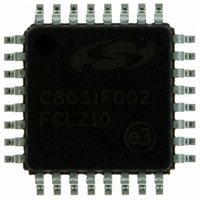
C8051F002-GQ Silicon Laboratories Inc, C8051F002-GQ Datasheet - Page 131

C8051F002-GQ
Manufacturer Part Number
C8051F002-GQ
Description
IC 8051 MCU 32K FLASH 32LQFP
Manufacturer
Silicon Laboratories Inc
Series
C8051F00xr
Specifications of C8051F002-GQ
Program Memory Type
FLASH
Program Memory Size
32KB (32K x 8)
Package / Case
32-LQFP
Core Processor
8051
Core Size
8-Bit
Speed
20MHz
Connectivity
SMBus (2-Wire/I²C), SPI, UART/USART
Peripherals
Brown-out Detect/Reset, POR, PWM, Temp Sensor, WDT
Number Of I /o
8
Ram Size
256 x 8
Voltage - Supply (vcc/vdd)
2.7 V ~ 3.6 V
Data Converters
A/D 4x12b; D/A 2x12b
Oscillator Type
Internal
Operating Temperature
-40°C ~ 85°C
Processor Series
C8051F0x
Core
8051
Data Bus Width
8 bit
Data Ram Size
256 B
Interface Type
I2C/SMBus/SPI/UART
Maximum Clock Frequency
20 MHz
Number Of Programmable I/os
8
Number Of Timers
4
Operating Supply Voltage
2.7 V to 3.6 V
Maximum Operating Temperature
+ 85 C
Mounting Style
SMD/SMT
3rd Party Development Tools
PK51, CA51, A51, ULINK2
Development Tools By Supplier
C8051F005DK
Minimum Operating Temperature
- 40 C
On-chip Adc
4-ch x 12-bit
On-chip Dac
2-ch x 12-bit
Package
32LQFP
Device Core
8051
Family Name
C8051F0xx
Maximum Speed
20 MHz
Lead Free Status / RoHS Status
Lead free / RoHS Compliant
For Use With
336-1246 - DEV KIT F300/301/302/303/304/305
Eeprom Size
-
Lead Free Status / Rohs Status
Lead free / RoHS Compliant
Other names
336-1186
Available stocks
Company
Part Number
Manufacturer
Quantity
Price
Company:
Part Number:
C8051F002-GQ
Manufacturer:
Silicon Laboratories Inc
Quantity:
10 000
Company:
Part Number:
C8051F002-GQR
Manufacturer:
Silicon Laboratories Inc
Quantity:
10 000
18.1.
The UART provides four operating modes (one synchronous and three asynchronous) selected by setting
configuration bits in the SCON register. These four modes offer different baud rates and communication protocols.
The four modes are summarized in Table 18.1 below. Detailed descriptions follow.
18.1.1. Mode 0: Synchronous Mode
Mode 0 provides synchronous, half-duplex communication. Serial data is transmitted and received on the RX pin.
The TX pin provides the shift clock for both transmit and receive. The MCU must be the master since it generates
the shift clock for transmission in both directions (see the interconnect diagram in Figure 18.2).
Eight data bits are transmitted/received, LSB first (see the timing diagram in Figure 18.3). Data transmission begins
when an instruction writes a data byte to the SBUF register. The TI Transmit Interrupt Flag (SCON.1) is set at the
end of the eighth bit time. Data reception begins when the REN Receive Enable bit (SCON.4) is set to logic 1 and
the RI Receive Interrupt Flag (SCON.0) is cleared. One cycle after the eighth bit is shifted in, the RI flag is set and
reception stops until software clears the RI bit. An interrupt will occur if enabled when either TI or RI is set.
The Mode 0 baud rate is the system clock frequency divided by twelve. RX is forced to open-drain in mode 0, and
an external pull-up will typically be required.
18.1.2. Mode 1: 8-Bit UART, Variable Baud Rate
131
C8051F000/1/2/5/6/7
C8051F010/1/2/5/6/7
Mode
0
1
2
3
UART Operational Modes
RX (data out)
RX (data in)
TX (clk out)
TX (clk out)
Synchronization
Asynchronous
Asynchronous
Asynchronous
Synchronous
Figure 18.3. UART Mode 0 Timing Diagram
C8051Fxxx
Figure 18.2. UART Mode 0 Interconnect
D0
D0
Timer 1 or Timer 2 Overflow
Timer 1 or Timer 2 Overflow
SYSCLK/32 or SYSCLK/64
Table 18.1. UART Modes
D1
RX
TX
D1
SYSCLK/12
Baud Clock
MODE 0 TRANSMIT
MODE 0 RECEIVE
Rev. 1.7
D2
D2
D3
CLK
DATA
D3
8 Extra Outputs
D4
D4
Data Bits
Reg.
Shift
D5
8
8
9
9
D5
D6
Start/Stop Bits
1 Start, 1 Stop
1 Start, 1 Stop
1 Start, 1 Stop
D6
None
D7
D7


