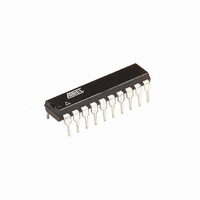
ATTINY261V-10PU Atmel, ATTINY261V-10PU Datasheet - Page 15

ATTINY261V-10PU
Manufacturer Part Number
ATTINY261V-10PU
Description
IC MCU AVR 2K FLASH 10MHZ 20-DIP
Manufacturer
Atmel
Series
AVR® ATtinyr
Datasheet
1.ATAVRMC321.pdf
(242 pages)
Specifications of ATTINY261V-10PU
Core Processor
AVR
Core Size
8-Bit
Speed
10MHz
Connectivity
USI
Peripherals
Brown-out Detect/Reset, POR, PWM, WDT
Number Of I /o
16
Program Memory Size
2KB (1K x 16)
Program Memory Type
FLASH
Eeprom Size
128 x 8
Ram Size
128 x 8
Voltage - Supply (vcc/vdd)
1.8 V ~ 5.5 V
Data Converters
A/D 11x10b
Oscillator Type
Internal
Operating Temperature
-40°C ~ 85°C
Package / Case
20-DIP (0.300", 7.62mm)
Package
20PDIP
Device Core
AVR
Family Name
ATtiny
Maximum Speed
10 MHz
Operating Supply Voltage
2.5|3.3|5 V
Data Bus Width
8 Bit
Number Of Programmable I/os
16
Interface Type
USI
On-chip Adc
11-chx10-bit
Number Of Timers
2
For Use With
ATSTK600 - DEV KIT FOR AVR/AVR32ATAVRBC100 - REF DESIGN KIT BATTERY CHARGER770-1007 - ISP 4PORT ATMEL AVR MCU SPI/JTAGATSTK505 - ADAPTER KIT FOR 14PIN AVR MCU
Lead Free Status / RoHS Status
Lead free / RoHS Compliant
Available stocks
Company
Part Number
Manufacturer
Quantity
Price
Company:
Part Number:
ATTINY261V-10PU
Manufacturer:
ATMEL
Quantity:
2 400
- Current page: 15 of 242
- Download datasheet (5Mb)
5. Memories
5.1
5.2
2588E–AVR–08/10
In-System Re-programmable Flash Program Memory
SRAM Data Memory
This section describes the different memories in the ATtiny261/461/861. The AVR architecture
has two main memory spaces, the Data memory and the Program memory space. In addition,
the ATtiny261/461/861 features an EEPROM Memory for data storage. All three memory
spaces are linear and regular.
The ATtiny261/461/861 contains 2/4/8K byte On-chip In-System Reprogrammable Flash mem-
ory for program storage. Since all AVR instructions are 16 or 32 bits wide, the Flash is organized
as 1024/2048/4096 x 16.
The Flash memory has an endurance of at least 10,000 write/erase cycles. The
ATtiny261/461/861 Program Counter (PC) is 10/11/12 bits wide, thus capable of addressing the
1024/2048/4096 Program memory locations.
detailed description on Flash data serial downloading using the SPI pins.
Constant tables can be allocated within the entire address space of program memory (see the
LPM – Load Program memory instruction description).
Timing diagrams for instruction fetch and execution are presented in
ing” on page
Figure 5-1.
Figure 5-2 on page 16
The lower data memory locations address both the Register File, the I/O memory and the inter-
nal data SRAM. The first 32 locations address the Register File, the next 64 locations the
standard I/O memory, and the last 128/256/512 locations address the internal data SRAM.
The five different addressing modes for the Data memory cover: Direct, Indirect with Displace-
ment, Indirect, Indirect with Pre-decrement, and Indirect with Post-increment. In the Register
File, registers R26 to R31 feature the indirect addressing pointer registers.
The direct addressing reaches the entire data space.
The Indirect with Displacement mode reaches 63 address locations from the base address given
by the Y- or Z-register.
11.
Program Memory Map
shows how the ATtiny261/461/861 SRAM Memory is organized.
Program Memory
“Memory Programming” on page 170
0x03FF/0x07FF/0x0FFF
0x0000
“Instruction Execution Tim-
contains a
15
Related parts for ATTINY261V-10PU
Image
Part Number
Description
Manufacturer
Datasheet
Request
R

Part Number:
Description:
Manufacturer:
Atmel Corporation
Datasheet:

Part Number:
Description:
Manufacturer:
Atmel Corporation
Datasheet:

Part Number:
Description:
IC MCU AVR 2K FLASH 20MHZ 32-QFN
Manufacturer:
Atmel
Datasheet:

Part Number:
Description:
IC MCU AVR 2K FLASH 20MHZ 20-DIP
Manufacturer:
Atmel
Datasheet:

Part Number:
Description:
MCU AVR 2K FLASH 15MHZ 32-QFN
Manufacturer:
Atmel
Datasheet:

Part Number:
Description:
MCU AVR 2KB FLASH 15MHZ 32-VQFN
Manufacturer:
Atmel
Datasheet:

Part Number:
Description:
IC MCU AVR 2K FLASH 20MHZ 20SOIC
Manufacturer:
Atmel
Datasheet:

Part Number:
Description:
Attiny261 8-bit Microcontroller With 2/4/8k Bytes In-system Programmable Flash
Manufacturer:
ATMEL Corporation
Datasheet:

Part Number:
Description:
IC MCU AVR 2K FLASH 20MHZ 20SOIC
Manufacturer:
Atmel
Datasheet:

Part Number:
Description:
IC MCU AVR 2K FLASH 20MHZ 32QFN
Manufacturer:
Atmel
Datasheet:


