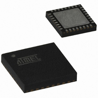
ATTINY261-20MU Atmel, ATTINY261-20MU Datasheet - Page 17

ATTINY261-20MU
Manufacturer Part Number
ATTINY261-20MU
Description
IC MCU AVR 2K FLASH 20MHZ 32-QFN
Manufacturer
Atmel
Series
AVR® ATtinyr
Specifications of ATTINY261-20MU
Core Processor
AVR
Core Size
8-Bit
Speed
20MHz
Connectivity
USI
Peripherals
Brown-out Detect/Reset, POR, PWM, WDT
Number Of I /o
16
Program Memory Size
2KB (1K x 16)
Program Memory Type
FLASH
Eeprom Size
128 x 8
Ram Size
128 x 8
Voltage - Supply (vcc/vdd)
2.7 V ~ 5.5 V
Data Converters
A/D 11x10b
Oscillator Type
Internal
Operating Temperature
-40°C ~ 85°C
Package / Case
32-VQFN Exposed Pad, 32-HVQFN, 32-SQFN, 32-DHVQFN
Processor Series
ATTINY2x
Core
AVR8
Data Bus Width
8 bit
Data Ram Size
128 B
Interface Type
2-Wire, SPI, USI
Maximum Clock Frequency
20 MHz
Number Of Programmable I/os
16
Number Of Timers
2
Maximum Operating Temperature
+ 85 C
Mounting Style
SMD/SMT
3rd Party Development Tools
EWAVR, EWAVR-BL
Development Tools By Supplier
ATAVRDRAGON, ATSTK500, ATSTK600, ATAVRISP2, ATAVRONEKIT
Minimum Operating Temperature
- 40 C
On-chip Adc
10 bit, 11 Channel
Package
32MLF EP
Device Core
AVR
Family Name
ATtiny
Maximum Speed
20 MHz
Operating Supply Voltage
3.3|5 V
For Use With
ATSTK600 - DEV KIT FOR AVR/AVR32ATAVRBC100 - REF DESIGN KIT BATTERY CHARGER770-1007 - ISP 4PORT ATMEL AVR MCU SPI/JTAGATSTK505 - ADAPTER KIT FOR 14PIN AVR MCU
Lead Free Status / RoHS Status
Lead free / RoHS Compliant
Available stocks
Company
Part Number
Manufacturer
Quantity
Price
Part Number:
ATTINY261-20MU
Manufacturer:
AVNET
Quantity:
20 000
5.3.1
5.3.2
5.3.3
5.3.4
5.3.5
2588E–AVR–08/10
EEPROM Read/Write Access
Atomic Byte Programming
Split Byte Programming
Erase
Write
The EEPROM Access Registers are accessible in the I/O space.
The write access times for the EEPROM are given in
tion, however, lets the user software detect when the next byte can be written. If the user code
contains instructions that write the EEPROM, some precautions must be taken. In heavily fil-
tered power supplies, V
device for some period of time to run at a voltage lower than specified as minimum for the clock
frequency used. See
problems in these situations.
In order to prevent unintentional EEPROM writes, a specific write procedure must be followed.
Refer to
details on this.
When the EEPROM is read, the CPU is halted for four clock cycles before the next instruction is
executed. When the EEPROM is written, the CPU is halted for two clock cycles before the next
instruction is executed.
Using Atomic Byte Programming is the simplest mode. When writing a byte to the EEPROM, the
user must write the address into the EEARL Register and data into EEDR Register. If the
EEPMn bits are zero, writing EEPE (within four cycles after EEMPE is written) will trigger the
erase/write operation. Both the erase and write cycle are done in one operation and the total
programming time is given in
and write operations are completed. While the device is busy with programming, it is not possi-
ble to do any other EEPROM operations.
It is possible to split the erase and write cycle in two different operations. This may be useful if
the system requires short access time for some limited period of time (typically if the power sup-
ply voltage falls). In order to take advantage of this method, it is required that the locations to be
written have been erased before the write operation. But since the erase and write operations
are split, it is possible to do the erase operations when the system allows doing time-critical
operations (typically after Power-up).
To erase a byte, the address must be written to EEAR. If the EEPMn bits are 0b01, writing the
EEPE within four cycles after EEMPE is written will trigger the erase operation only (program-
ming time is given in
completes. While the device is busy programming, it is not possible to do any other EEPROM
operations.
To write a location, the user must write the address into EEAR and the data into EEDR. If the
EEPMn bits are 0b10, writing the EEPE (within four cycles after EEMPE is written) will trigger
the write operation only (programming time is given in
remains set until the write operation completes. If the location to be written has not been erased
before write, the data that is stored must be considered as lost. While the device is busy with
programming, it is not possible to do any other EEPROM operations.
“Atomic Byte Programming” on page 17
Table 5-1 on page
“Preventing EEPROM Corruption” on page 19
CC
is likely to rise or fall slowly on Power-up/down. This causes the
Table 5-1 on page
22). The EEPE bit remains set until the erase operation
and
22. The EEPE bit remains set until the erase
Table 5-1 on page
“Split Byte Programming” on page 17
Table 5-1 on page
for details on how to avoid
22. A self-timing func-
22). The EEPE bit
for
17


