ATTINY13A-MU Atmel, ATTINY13A-MU Datasheet - Page 81
ATTINY13A-MU
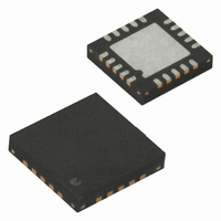
Manufacturer Part Number
ATTINY13A-MU
Description
IC MCU AVR 1K FLASH 20MHZ 20-QFN
Manufacturer
Atmel
Series
AVR® ATtinyr
Specifications of ATTINY13A-MU
Core Processor
AVR
Core Size
8-Bit
Speed
20MHz
Peripherals
Brown-out Detect/Reset, POR, PWM, WDT
Number Of I /o
6
Program Memory Size
1KB (512 x 16)
Program Memory Type
FLASH
Eeprom Size
64 x 8
Ram Size
64 x 8
Voltage - Supply (vcc/vdd)
1.8 V ~ 5.5 V
Data Converters
A/D 4x10b
Oscillator Type
Internal
Operating Temperature
-40°C ~ 85°C
Package / Case
20-MLF®, QFN
Processor Series
ATTINY1x
Core
AVR8
Data Bus Width
8 bit
Data Ram Size
64 B
Interface Type
SPI
Maximum Clock Frequency
20 MHz
Number Of Programmable I/os
6
Number Of Timers
1
Maximum Operating Temperature
+ 85 C
Mounting Style
SMD/SMT
3rd Party Development Tools
EWAVR, EWAVR-BL
Development Tools By Supplier
ATAVRDRAGON, ATSTK500, ATSTK600, ATAVRISP2, ATAVRONEKIT, ATAKSTK511
Minimum Operating Temperature
- 40 C
On-chip Adc
10 bit, 4 Channel
For Use With
ATSTK600-DIP40 - STK600 SOCKET/ADAPTER 40-PDIP770-1007 - ISP 4PORT ATMEL AVR MCU SPI/JTAGATAVRDRAGON - KIT DRAGON 32KB FLASH MEM AVRATAVRISP2 - PROGRAMMER AVR IN SYSTEMATJTAGICE2 - AVR ON-CHIP D-BUG SYSTEM
Lead Free Status / RoHS Status
Lead free / RoHS Compliant
Connectivity
-
Lead Free Status / Rohs Status
Lead free / RoHS Compliant


13.2.3
8126E–AVR–07/10
DIDR0 – Digital Input Disable Register 0
• Bits 1:0 – ACIS[1:0]: Analog Comparator Interrupt Mode Select
These bits determine which comparator events that trigger the Analog Comparator interrupt. The
different settings are shown in
Table 13-2.
When changing the ACIS1/ACIS0 bits, the Analog Comparator Interrupt must be disabled by
clearing its Interrupt Enable bit in the ACSR Register. Otherwise an interrupt can occur when the
bits are changed.
• Bits 1:0 – AIN1D, AIN0D: AIN[1:0] Digital Input Disable
When this bit is written logic one, the digital input buffer on the AIN1/0 pin is disabled. The corre-
sponding PIN Register bit will always read as zero when this bit is set. When an analog signal is
applied to the AIN1/0 pin and the digital input from this pin is not needed, this bit should be writ-
ten logic one to reduce power consumption in the digital input buffer.
Bit
0x14
Read/Write
Initial Value
ACIS1
0
0
1
1
ACIS1/ACIS0 Settings
R
7
–
0
ACIS0
0
1
0
1
6
–
R
0
Interrupt Mode
Comparator Interrupt on Output Toggle.
Reserved
Comparator Interrupt on Falling Output Edge.
Comparator Interrupt on Rising Output Edge.
Table 13-2 on page
ADC0D
R/W
5
0
ADC2D
R/W
4
0
81.
ADC3D
R/W
3
0
ADC1D
R/W
2
0
AIN1D
R/W
1
0
AIN0D
R/W
0
0
DIDR0
81
Related parts for ATTINY13A-MU
Image
Part Number
Description
Manufacturer
Datasheet
Request
R

Part Number:
Description:
IC MCU AVR 1K FLASH 20MHZ 8SOIC
Manufacturer:
Atmel
Datasheet:

Part Number:
Description:
Manufacturer:
Atmel Corporation
Datasheet:
Part Number:
Description:
IC MCU AVR 1K FLASH 20MHZ 8SOIC
Manufacturer:
Atmel
Datasheet:

Part Number:
Description:
IC MCU AVR 1K FLASH 10MHZ 20-MLF
Manufacturer:
Atmel
Datasheet:

Part Number:
Description:
IC MCU AVR 1K FLASH 20MHZ 8DIP
Manufacturer:
Atmel
Datasheet:

Part Number:
Description:
MCU AVR 1KB FLASH 20MHZ 3X3 QFN
Manufacturer:
Atmel
Datasheet:
Part Number:
Description:
IC MCU AVR 1K FLASH 20MHZ 8SOIC
Manufacturer:
Atmel
Datasheet:
Part Number:
Description:
IC MCU AVR 1K 5V 20MHZ 8DIP
Manufacturer:
Atmel
Datasheet:
Part Number:
Description:
IC MCU AVR 1K 5V 20MHZ 8SOIC
Manufacturer:
Atmel
Datasheet:
Part Number:
Description:
IC MCU AVR 1K 5V 20MHZ 8SOIC
Manufacturer:
Atmel
Datasheet:
Part Number:
Description:
IC MCU AVR 1K FLASH 20MHZ 8DIP
Manufacturer:
Atmel
Datasheet:
Part Number:
Description:
IC MCU AVR 1K FLASH 20MHZ 8SOIC
Manufacturer:
Atmel
Datasheet: