MC74LCX16245DT ON Semiconductor, MC74LCX16245DT Datasheet

Bus Transceivers Low Voltage CMOS

MC74LCX16245DT

Manufacturer Part Number
MC74LCX16245DT
Description
Bus Transceivers Low Voltage CMOS
Manufacturer
ON Semiconductor
Datasheet

Specifications of MC74LCX16245DT

Logic Type
CMOS
Logic Family
74LCX
Number Of Channels Per Chip
16
Input Level
LVTTL, TTL
Output Level
LVCMOS
Output Type
3-State
High Level Output Current
- 24 mA
Low Level Output Current
24 mA
Propagation Delay Time
5.2 ns
Supply Voltage (max)
3.6 V
Supply Voltage (min)
2 V
Maximum Operating Temperature
+ 85 C
Package / Case
TSSOP-48
Function
Bus Transceiver
Maximum Power Dissipation
200 mW
Minimum Operating Temperature
- 40 C
Mounting Style
SMD/SMT
Number Of Circuits
2
Polarity
Non-Inverting
Lead Free Status / Rohs Status
No RoHS Version Available

Available stocks

Company
Part Number
Manufacturer
Quantity
Price
Part Number:
MC74LCX16245DT
Manufacturer:
MOT
Quantity:
6 227
Part Number:
MC74LCX16245DTG
Manufacturer:
ON Semiconductor
Quantity:
1
Part Number:
MC74LCX16245DTG
Manufacturer:
ON/安森美
Quantity:
20 000
Company:
Part Number:
MC74LCX16245DTG
Quantity:
6 000
Part Number:
MC74LCX16245DTR2
Manufacturer:
ON/安森美
Quantity:
20 000
Part Number:
MC74LCX16245DTR2G
Manufacturer:
NXP
Quantity:
12 000
Part Number:
MC74LCX16245DTR2G
Manufacturer:
ON/安森美
Quantity:
20 000
Part Number:
MC74LCX16245DTRG
Manufacturer:
ONSemi
Quantity:
6 876
MC74LCX16245
Low−Voltage CMOS
16−Bit Transceiver
With 5 V−Tolerant Inputs and Outputs
(3−State, Non−Inverting)
transceiver operating from a 2.3 to 3.6 V supply. The device is byte
controlled. Each byte has separate Output Enable inputs which can be
tied together for full 16−bit operation. High impedance TTL
compatible inputs significantly reduce current loading to input drivers
while TTL compatible outputs offer improved switching noise
performance. A V
inputs to be safely driven from 5.0 V devices. The MC74LCX16245 is
suitable for memory address driving and all TTL level bus oriented
transceiver applications.
applications. Current drive capability is 24 mA at both A and B ports.
The Transmit/Receive (T/Rn) inputs determine the direction of data
flow through the bidirectional transceiver. Transmit (active−HIGH)
enables data from A ports to B ports; Receive (active−LOW) enables
data from B to A ports. The Output Enable inputs (OEn), when HIGH,
disable both A and B ports by placing them in a HIGH Z condition.
Features
*For additional information on our Pb−Free strategy and soldering details, please
© Semiconductor Components Industries, LLC, 2005
August, 2005 − Rev. 7
download the ON Semiconductor Soldering and Mounting Techniques
Reference Manual, SOLDERRM/D.
The MC74LCX16245 is a high performance, non−inverting 16−bit
The 4.5 ns maximum propagation delays support high performance
Substantially Reduces System Power Requirements
Designed for 2.3 to 3.6 V V
4.5 ns Maximum t
5.0 V Tolerant − Interface Capability With 5.0 V TTL Logic
Supports Live Insertion and Withdrawal
I
LVTTL Compatible
LVCMOS Compatible
24 mA Balanced Output Sink and Source Capability
Near Zero Static Supply Current in All Three Logic States (20 mA)
Latchup Performance Exceeds 500 mA
ESD Performance: Human Body Model >2000 V;
These are Pb−Free Devices*
OFF
Specification Guarantees High Impedance When V
I
specification of 5.5 V allows MC74LCX16245
pd
Machine Model >200 V
CC
Operation
CC
1
= 0 V
See detailed ordering and shipping information in the package
dimensions section on page 3 of this data sheet.
48
ORDERING INFORMATION
A
WL
YY
WW
G
48
1
MARKING DIAGRAM
1
http://onsemi.com
LCX16245G
= Assembly Location
= Wafer Lot
= Year
= Work Week
= Pb−Free Package
AWLYYWW
Publication Order Number:
CASE 1201
DT SUFFIX
TSSOP−48
MC74LCX16245/D

Related parts for MC74LCX16245DT

MC74LCX16245DT Summary of contents

Page 1

... ESD Performance: Human Body Model >2000 V; Machine Model >200 V • These are Pb−Free Devices* *For additional information on our Pb−Free strategy and soldering details, please download the ON Semiconductor Soldering and Mounting Techniques Reference Manual, SOLDERRM/D. © Semiconductor Components Industries, LLC, 2005 August, 2005 − Rev. 7 http://onsemi.com ...

Page 2

T/ GND GND GND 15 B10 16 B11 B12 19 ...

Page 3

... ORDERING INFORMATION Device MC74LCX16245DT MC74LCX16245DTG MC74LCX16245DTR2 M74LCX16245DTR2G †For information on tape and reel specifications, including part orientation and tape sizes, please refer to our Tape and Reel Packaging Specifications Brochure, BRD8011/D. *This package is inherently Pb−Free. MAXIMUM RATINGS Symbol Parameter V DC Supply Voltage Input Voltage ...

Page 4

DC ELECTRICAL CHARACTERISTICS Symbol Characteristic V HIGH Level Input Voltage (Note LOW Level Input Voltage (Note HIGH Level Output Voltage OH V LOW Level Output Voltage OL I Input Leakage Current I I 3−State ...

Page 5

DYNAMIC SWITCHING CHARACTERISTICS Symbol Characteristic V Dynamic LOW Peak Voltage OLP (Note 4) V Dynamic LOW Valley Voltage OLV (Note 4) 4. Number of outputs defined as “n”. Measured with “n−1” outputs switching from HIGH−to−LOW or LOW−to−HIGH. The remaining output ...

Page 6

Vmi An PHL Vmo Bn, An WAVEFORM 1 − PROPAGATION DELAYS 2.5 ns, 10 MHz Table 2. AC WAVEFORMS Symbol Vmi Vmo ...

Page 7

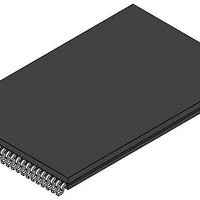
K 48X REF 0.12 (0.005 PIN 1 IDENT. −V− 0.076 (0.003) −T− SEATING PLANE G MC74LCX16245 PACKAGE DIMENSIONS TSSOP−48 DT SUFFIX CASE 1201−01 ISSUE Ç ...

Page 8

... Fax: 480−829−7709 or 800−344−3867 Toll Free USA/Canada Email: orderlit@onsemi.com MC74LCX16245 N. American Technical Support: 800−282−9855 Toll Free USA/Canada Japan: ON Semiconductor, Japan Customer Focus Center 2−9−1 Kamimeguro, Meguro−ku, Tokyo, Japan 153−0051 Phone: 81−3−5773−3850 http://onsemi.com 8 ON Semiconductor Website: http://onsemi ...

Related keywords