EVAL6730 STMicroelectronics, EVAL6730 Datasheet - Page 43
EVAL6730
Manufacturer Part Number
EVAL6730
Description
EVAL BOARD FOR L6730XX
Manufacturer
STMicroelectronics
Type
Motor / Motion Controllers & Driversr
Datasheets
1.L6730TR.pdf
(52 pages)
2.L6730DTR.pdf
(50 pages)
3.EVAL6730.pdf
(9 pages)
4.EVAL6732.pdf
(43 pages)
Specifications of EVAL6730
Main Purpose
DC/DC, Step Down
Outputs And Type
1, Non-Isolated
Power - Output
66W
Voltage - Output
3.3V
Current - Output
20A
Voltage - Input
4.5 ~ 14V
Regulator Topology
Buck
Frequency - Switching
400kHz
Board Type
Fully Populated
Utilized Ic / Part
L6730
Input Voltage
8 V to 52 V
Product
Power Management Modules
Lead Free Status / RoHS Status
Lead free / RoHS Compliant
For Use With/related Products
L6208
Other names
497-5501
Available stocks
Company
Part Number
Manufacturer
Quantity
Price


L6730 - L6730B
8
I/O Description
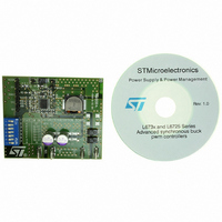
Figure 38. Demonstration board
Table 11.
Output (V
Input (Vin-Gin)
V
CC
Symbol
V
-GND
TP1
CCDR
OUT
-G
I/O functions
CC
OUT
)
The input voltage can range from 1.8V to 14V. If the input voltage is between
4.5V and 14V it can supply also the device (through the V
case the pin 1 and 2 of the jumper G1 must be connected together.
The output voltage is fixed at 3.3V but it can be changed by replacing the
resistor R14 of the output resistor divider:
The over-current-protection limit is set at 15A but it can be changed by
replacing the resistors R1 and R12 (see OCL and OCH pin in
connection).
Using the input voltage to supply the controller no power is required at this
input. However the controller can be supplied separately from the power stage
through the V
open.
An internal LDO provides the power into the device. The input of this stage is
the V
providing directly a 5V voltage from V
and 3 of the jumper G1 must be shorted.
This pin can be used as an input or as a test point. If all the jumper G2 pins are
shorted, TP1 can be used as a test point of the voltage at the EAREF pin. If
the pins 2 and 3 of G2 are connected together, TP1 can be used as an input to
provide an external reference for the internal error amplifier (see section 4.3.
Internal and external references).
CC
pin and the output (5V) is the V
Doc ID 11938 Rev 3
CC
input (4.5-14V) and, in this case, jumper G1 must be left
Vo
=
V
REF
Function
⋅
CCDR
1 (
CCDR
+
R
R
and Gndcc. In this case the pins 1
16
14
)
pin. The LDO can be bypassed,
CC
pin) and in this
I/O Description
Table 4: Pin
43/52
Related parts for EVAL6730
Image
Part Number
Description
Manufacturer
Datasheet
Request
R

Part Number:
Description:
STMicroelectronics [RIPPLE-CARRY BINARY COUNTER/DIVIDERS]
Manufacturer:
STMicroelectronics
Datasheet:
Part Number:
Description:
STMicroelectronics [LIQUID-CRYSTAL DISPLAY DRIVERS]
Manufacturer:
STMicroelectronics
Datasheet:

Part Number:
Description:
BOARD EVAL FOR MEMS SENSORS
Manufacturer:
STMicroelectronics
Datasheet:
Part Number:
Description:
NPN TRANSISTOR POWER MODULE
Manufacturer:
STMicroelectronics
Datasheet:
Part Number:
Description:
TURBOSWITCH ULTRA-FAST HIGH VOLTAGE DIODE
Manufacturer:
STMicroelectronics
Datasheet:
Part Number:
Description:
Manufacturer:
STMicroelectronics
Datasheet:
Part Number:
Description:
DIODE / SCR MODULE
Manufacturer:
STMicroelectronics
Datasheet:
Part Number:
Description:
DIODE / SCR MODULE
Manufacturer:
STMicroelectronics
Datasheet:
Part Number:
Description:
Search -----> STE16N100
Manufacturer:
STMicroelectronics
Datasheet:
Part Number:
Description:
Search ---> STE53NA50
Manufacturer:
STMicroelectronics
Datasheet:
Part Number:
Description:
NPN Transistor Power Module
Manufacturer:
STMicroelectronics
Datasheet:
Part Number:
Description:
DIODE / SCR MODULE
Manufacturer:
STMicroelectronics
Datasheet: