AD8336-EVALZ Analog Devices Inc, AD8336-EVALZ Datasheet
AD8336-EVALZ
Specifications of AD8336-EVALZ
Available stocks


Related parts for AD8336-EVALZ


AD8336-EVALZ Summary of contents
Page 1
... high temperatures. The operating temperature range is −55°C to +125°C. The AD8336 is available in a 16-lead LFCSP (4 mm × 4 mm). One Technology Way, P.O. Box 9106, Norwood, MA 02062-9106, U.S.A. Tel: 781.329.4700 Fax: 781.461.3113 © ...
Page 2
... AD8336 TABLE OF CONTENTS Features .............................................................................................. 1 Applications ....................................................................................... 1 Functional Block Diagram .............................................................. 1 General Description ......................................................................... 1 Revision History ............................................................................... 2 Specifications ..................................................................................... 3 Absolute Maximum Ratings ............................................................ 5 ESD Caution .................................................................................. 5 Pin Configuration and Function Descriptions ............................. 6 Typical Performance Characteristics ............................................. 7 Test Circuits ..................................................................................... 16 Theory of Operation ...................................................................... 20 Overview ...................................................................................... 20 Preamplifier ................................................................................. 20 REVISION HISTORY 9/08—Rev Rev. A Change to General Description Section ........................................ 1 Deleted Input Capacitance Parameter, Table 1 ...
Page 3
... AD8336 1 Unit MHz MHz nA μV kΩ pF MHz MHz MHz MHz MHz MHz MHz MHz V/μs nV/√Hz pA/√Hz nV/√Hz nV/√Hz nV/√Hz nV/√Hz nV/√Hz nV/√ ...
Page 4
... AD8336 Parameter 2 ABSOLUTE GAIN ERROR GAIN CONTROL INTERFACE Gain Scaling Factor Intercept Gain Range Input Voltage (V ) Range GAIN Input Current Response Time OUTPUT PERFORMANCE Output Impedance MHz Output Signal Swing Output Current Short-Circuit Current Output Offset Voltage PWRA PIN Normal Power (Logic Low) ...
Page 5
... W 1.12 W ESD CAUTION –55°C to +125°C –55°C to +85°C –65°C to +150°C 300°C 58.2°C/W 35.9°C/W 9.2°C/W 1.1°C/W 34.5°C/W Rev Page AD8336 ...
Page 6
... No Connect Connect Connect VOUT GNEG 1 12 PIN 1 INDICATOR PWRA GPOS 2 11 AD8336 VCOM VNEG 3 10 TOP VIEW (Not to Scale) INPP VGAI NOTES CONNECT 2. THE EXPOSED PAD IS NOT CONNECTED INTERNALLY. FOR INCREASED RELIABILITY OF THE SOLDER JOINTS AND MAXIMUM THERMAL CAPABILITY RECOMMENDED THAT THE PADDLE BE SOLDERED TO THE GROUND PLANE ...
Page 7
... V (mV) GAIN Figure 8. Gain Error vs. V for Preamp Gains of 4× and 20× GAIN (See Figure 56) AD8336 T = +125° +25° –55°C 600 800 V = ±12V ± ±3V S 600 800 ) S 600 ...
Page 8
... AD8336 2.0 PREAMP GAIN = 4× 1MHz PREAMP GAIN = 4× 10MHz 1.5 PREAMP GAIN = 20× 1MHz PREAMP GAIN = 20× 10MHz 1.0 0.5 0 –0.5 –1.0 –1.5 –2.0 –800 –600 –400 –200 0 200 V (mV) GAIN Figure 9. Gain Error vs MHz and 10 MHz and GAIN for Preamp Gains of 4× and 20× ...
Page 9
... Figure 19. Frequency Response for Various Values PREAMP GAIN = 20× –10 100k 16.55 Figure 20. Frequency Response for Various Values of V Rev Page AD8336 V = +0.7V GAIN +0.5V +0.2V 0V –0.2V –0.5V –0.7V 1M 10M 100M 200M FREQUENCY (Hz) GAIN (See Figure 57 +0.7V GAIN +0 ...
Page 10
... AD8336 +0.7V GAIN +0. +0. –0.2V 0 –0.5V –10 –0.7V –20 PREAMP GAIN = –3× –30 100k 1M 10M FREQUENCY (Hz) Figure 21. Frequency Response for Various Values of V When the Preamp Gain is −3× (See Figure 69 and Figure 57 GAIN 47pF 22pF L – 10pF 0pF L –10 ...
Page 11
... Preamp Gains of 4× and 20× GAIN (See Figure 62 0.7V GAIN 10M FREQUENCY (Hz) for Three Values of Power Supply Voltage (V (See Figure 0.7V GAIN 1M 10M FREQUENCY (Hz) at Maximum Inverting Gain (See Figure 73) AD8336 f = 5MHz 600 800 = ±12V S = ± ±3V S 100M ) S 100M ...
Page 12
... AD8336 100 V = 0.7V GAIN 10 INPUT-REFERRED NOISE R THERMAL NOISE ALONE 1 S 0.1 10 100 SOURCE RESISTANCE (Ω) Figure 33. Input-Referred Noise vs. Source Resistance (See Figure 72 SIMULATED DATA –800 –600 –400 –200 0 200 V (mV) GAIN Figure 34. Noise Figure vs. V (See Figure 63) – p-p OUT GAIN f = 5MHz – ...
Page 13
... Two Frequencies and Two Input Levels (see Figure 76) INPUT LEVEL LIMITED BY GAIN OF PREAMP V = ±12V ± ±3V S –600 –400 –200 0 200 400 600 V (mV) GAIN at Three Power Supply Values (V GAIN (see Figure 74 and Figure 75 (V) OUT 0 100 200 300 TIME (ns) (See Figure 65) AD8336 800 800 ) S ...
Page 14
... AD8336 0 0.7V GAIN 0.4 0.2 0 –0.2 –0.4 INPUT OUTPUT WHEN PWRA = 0 OUTPUT WHEN PWRA = 1 –0.6 –100 – 100 150 200 TIME (ns) Figure 45. Noninverting Small-Signal Pulse Response for Both Power Levels (See Figure 65) 0.6 OUTPUT 0 0.7V GAIN PREAMP GAIN = –3× 0.2 0 – ...
Page 15
... Rev Page PSRR V POS NEG V = 0.7V GAIN GAIN V = –0.7V GAIN 1M FREQUENCY (Hz) (See Figure 71) HIGH POWER LOW POWER V = ±12V ± ±3V S –45 –25 – 115 TEMPERATURE (°C) vs. Temperature for Three Values of Supply Voltage Q and High and Low Power (See Figure 68) AD8336 5M GAIN 135 ...
Page 16
... Rev Page NETWORK ANALYZER OUT IN 50Ω 50Ω AD8336 + 4 PrA 1 49.9Ω – 301Ω 100Ω Figure 59. Group Delay AD8336 + 4 453Ω PrA 1 – 5 DMM 301Ω ¯ 100Ω Figure 60. Offset Voltage NETWORK ANALYZER CONFIGURE TO MEASURE Z-CONVERTED S22 IN 50Ω ...
Page 17
... DIFFERENTIAL 11 FET PROBE AD8336 453Ω PrA 1 – 301Ω 100Ω Figure 66. Gain Response OSCILLOSCOPE –20dB CH1 CH2 POWER SPLITTER 50Ω 50Ω AD8336 + 453Ω 4 PrA 1 – 301Ω 0.7V 100Ω Figure 67. VGA Overdrive Recovery AD8336 NC NC ...
Page 18
... VPOS OR VNEG AD8336 4 + PrA 1 49.9Ω – DIFFERENTIAL 301Ω V GAIN 100Ω Figure 71. Power Supply Rejection Ratio SPECTRUM ANALYZER IN 50Ω AD8336 + 4 PrA 1 – 301Ω 0.7V 100Ω Figure 72. Input-Referred Noise vs. Source Resistance SPECTRUM ANALYZER IN 50Ω AD8336 4 + PrA 1 – ...
Page 19
... GAIN SPECTRUM ANALYZER IN 50Ω AD8336 DUT 453Ω 0Ω PrA 1 – 301Ω V GAIN 100Ω , High Signal Level Inputs GAIN SPECTRUM ANALYZER INPUT 50Ω AD8336 DUT 453Ω PrA 1 49.9Ω – 301Ω V GAIN 100Ω AD8336 –20dB ...
Page 20
... If desired, the op amp output (PRAO) and VGA input (VGAI) pins provide for connection of an interstage filter to eliminate noise and offset. The bandwidth of the AD8336 100 MHz with a gain range (− +46 dB). For applications that require large supply voltages, a reduction in power is advantageous ...
Page 21
... FB2 VGA Using the values listed in Table 4, the total noise of the AD8336 is slightly less than 3 nV/√Hz, referred to the input. Although the input noise referred to the VGA is 3.1 nV/√Hz, the input- referred noise at the preamp is 0.77 nV/√Hz when divided by the preamplifier gain of 4× ...
Page 22
... At higher preamplifier gains, the bandwidth diminishes proportionally in conformance to the classical voltage gain amplifier GBW relationship. While setting the overall gain of the AD8336, the user needs to consider the input-referred offset voltage of the preamplifier. Although the offset of the attenuator and postamplifier are ...
Page 23
... MHz. The voltage at Pin PWRA must not exceed 5 V. DRIVING CAPACITIVE LOADS The output stages of the AD8336 are stable with capacitive loads for a supply voltage of ±3 V and with capacitive loads for supply voltages up to ±8 V. For larger combined values of load capacitance and/or supply voltage Ω series resistor is recommended for stability ...
Page 24
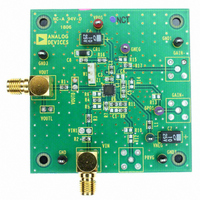
... AD8336 EVALUATION BOARD An evaluation board, AD8336-EVALZ, is available online for the AD8336. Figure photo of the board. The board is shipped from the factory configured for a preamp gain of 4×. To change the value of the gain of the preamp or to change the gain polarity to inverting, alter the component values or install components in the alternate locations provided ...
Page 25
... Figure 84. Component Side Copper Figure 85. Secondary Side Copper Figure 86. Component Side Silk Screen Figure 87. Internal Ground Plane Copper Figure 88. Internal Power Plane Copper Rev Page AD8336 ...
Page 26
... CR1 C8 5.1V 0.1µF R3 VIN 0Ω VIN1 R2 49.9Ω CONNECT Figure 89. AD8336-EVALZ Schematic Shown as Shipped, Configured for a Noninverting Gain of 4× Table 6. AD8336 Evaluation Board Bill of Materials Qty Name Description 2 Capacitor Tantalum 10 μ Capacitor 0.1 μ 0603, X7R 1 Capacitor ...
Page 27
... ORDERING GUIDE Model Temperature Range 1 AD8336ACPZ-R7 −40°C to +85°C AD8336ACPZ-RL 1 −40°C to +85°C 1 AD8336ACPZ-WP −40°C to +85°C 1 AD8336-EVALZ RoHS Compliant Part. 4.00 BSC SQ 0.60 MAX 0.65 BSC TOP 3.75 VIEW BSC SQ 0.75 0.60 0.50 0.80 MAX ...
Page 28
... AD8336 NOTES ©2006–2008 Analog Devices, Inc. All rights reserved. Trademarks and registered trademarks are the property of their respective owners. D06228-0-9/08(A) Rev Page ...