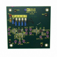
AD8231-EVALZ Analog Devices Inc, AD8231-EVALZ Datasheet
AD8231-EVALZ
Specifications of AD8231-EVALZ
Available stocks


Related parts for AD8231-EVALZ


AD8231-EVALZ Summary of contents
Page 1
... AD8224 1 Rail-to-rail output. The AD8231 also includes an uncommitted op amp that can be used for additional gain, differential signal driving, or filtering. Like the in-amp, the op amp has an auto-zero architecture, rail- to-rail input, and rail-to-rail output. The AD8231 includes a shutdown feature that reduces current to a maximum of 1 μ ...
Page 2
... Inserted Figure 48; Renumbered Sequentially............................ 17 Changes to Gain Selection Section and Figure 50 ..................... 18 Added Input Protection Section................................................... 19 Added Reducing Noise Section .................................................... 20 Changes to Multiplexing Section.................................................. 21 Added Using the AD8231 with Bipolar Supplies Section ......... 21 Added Sallen Key Filter Section ................................................... 22 Changes to Ordering Guide .......................................................... 23 Amplifier Architecture .............................................................. 18 Gain Selection............................................................................. 18 Reference Terminal ...
Page 3
... 2 IN+ IN− kHz kHz −40° kHz 125° 0 kHz kHz −40° kHz 125° 0 Rev Page AD8231 Min Typ Max Unit 4 15 μV 0.01 0.05 μV/° μV 0.05 0.5 μV/°C 250 500 100 pA 0.5 nA 0.05 % 0.8 ...
Page 4
... AD8231 Parameter Dynamic Performance Bandwidth Gain Bandwidth Product 128 Slew Rate Output Characteristics Output Voltage High Output Voltage Low Short-Circuit Current Digital Interface Input Voltage Low Input Voltage High Setup Time to CS High Hold Time after CS High OPERATIONAL AMPLIFIER Input Characteristics ...
Page 5
... 2 25°C IN+ IN− kHz kHz −40° kHz 125° 0 kHz kHz −40° kHz 125° 0 Rev Page AD8231 Min Typ Max Unit 4 15 μV 0.01 0.05 μV/° μV 0.05 0.5 μV/°C 250 500 100 pA 0 ...
Page 6
... AD8231 Parameter Dynamic Performance Bandwidth Gain Bandwidth Product 128 Slew Rate Output Characteristics Output Voltage High Output Voltage Low Short-Circuit Current Digital Interface Input Voltage Low Input Voltage High Setup Time to CS High Hold Time after CS High OPERATIONAL AMPLIFIERS Input Characteristics ...
Page 7
... MAXIMUM POWER DISSIPATION 0.2 kV The maximum safe power dissipation for the AD8231 is limited by the associated rise in junction temperature (T approximately 130°C, which is the glass transition temperature, the plastic changes its properties. Even temporarily exceeding this temperature limit may change the stresses that the package exerts on the die, permanently shifting the parametric perform- ance of the amplifiers. Exceeding a temperature of 130° ...
Page 8
... PIN INDICATOR S (IN-AMP –IN) –INA 2 11 –V AD8231 S (IN-AMP +IN) +INA 3 10 OUTA (IN-AMP OUT) TOP VIEW (Not to Scale REF CONNECT Figure 2. Pin Configuration Description No Connect. Instrumentation Amplifier Negative Input. Instrumentation Amplifier Positive Input. No Connect. Shutdown. Operational Amplifier Positive Input. Operational Amplifier Negative Input. ...
Page 9
... INPUT OFFSET DRIFT (nV/°C) Figure 7. Instrumentation Amplifier Input Offset Voltage Drift, −40°C to +125° MEAN: –0.003 14 SD: 0.061 –0.5 –0.4 –0.3 –0.2 –0.1 0 0.1 0.2 OUTPUT OFFSET DRIFT (µV/°C) AD8231 300 400 500 0.3 0.4 0.5 ...
Page 10
... AD8231 2000 V = MIDSUPPLY REF V = MIDSUPPLY CM 1500 1000 500 –500 –40 – TEMPERATURE (°C) Figure 9. Instrumentation Amplifier Bias Current vs. Temperature 2.0 1.5 1.0 0.5 0 –0.5 –1.0 –1.5 –2.0 –2.5 –2.0 –1.5 –1.0 –0.5 0 0.5 V (V) CM Figure 10. Instrumentation Amplifier Bias Current vs. Common-Mode Voltage ...
Page 11
... Figure 19. Instrumentation Amplifier Positive PSRR vs. Frequency 140 120 100 10k 100k 1 Figure 20. Instrumentation Amplifier Negative PSRR vs. Frequency Rev Page REPRESENTATIVE SAMPLES – 100 TEMPERATURE (° 128 10 100 1k 10k FREQUENCY (Hz 128 10 100 1k 100k FREQUENCY (Hz) AD8231 128 G = 128 120 100k 100k ...
Page 12
... AD8231 G = +128, 0.4µV/DIV G = +1, 1µV/DIV Figure 21. Instrumentation Amplifier 0 Noise 100 +128 FREQUENCY (Hz) Figure 22. Instrumentation Amplifier Voltage Noise Spectral Density vs. Frequency 1000 Hz 1000 900 G = +128 800 700 600 500 400 300 200 100 100 1k FREQUENCY (Hz) Figure 23. Instrumentation Amplifier Voltage Noise Spectral Density vs. ...
Page 13
... Figure 30. Instrumentation Amplifier Large Signal Pulse Response 10µs/DIV Figure 31. Instrumentation Amplifier Settling Time vs 10µs/DIV Figure 32. Instrumentation Amplifier Settling Time vs. Rev Page AD8231 17.6µs TO 0.01% 21.4µs TO 0.001% 100µs/DIV G = 128 0.001% 0.01% 10 100 1 k GAIN (V/V) Gain for p-p Step 0.001% 0.01% 10 ...
Page 14
... AD8231 +V S –0.2 –0.4 –0.6 –0.8 –1.0 1.0 0.8 0.6 0.4 0.2 –V S 0.1 1 OUTPUT CURRENT (mA) Figure 33. Instrumentation Amplifier Output Voltage Swing vs. Output Current –40°C +25°C +85°C +125°C 10 100 Figure 34. Instrumentation Amplifier Output Voltage Swing vs. Rev Page –0.2 –0.4 – ...
Page 15
... Figure 40. Operational Amplifier Large Signal Transient Response Rev Page LOAD 300pF 800pF 1nF 1.5nF 20mV/DIV 5µs/DIV Figure 38. Operational Amplifier Small Signal Response for Various Capacitive Loads LOAD 1nF║2kΩ 1.5nF║2kΩ TIME (5µs/DIV) NO LOAD 1nF║2kΩ 1.5nF║2kΩ TIME (5µs/DIV) AD8231 = ...
Page 16
... AD8231 1000 900 800 700 600 500 400 300 200 100 100 1k FREQUENCY (Hz) Figure 41. Operational Amplifier Voltage Spectral Noise Density vs. Frequency 2.2 2.0 1.8 1.6 1.4 1.2 1.0 0.8 0.6 0.4 0 –0.2 –40 –25 – TEMPERATURE (°C) Figure 42. Operational Amplifier Bias Current vs. Temperature ...
Page 17
... V (V) SUPPLY Figure 47. Supply Current vs. Supply Voltage 160 +125°C 140 +85°C 120 +25°C 100 –40° 5.1 5.5 5.9 Rev Page 128 SOURCE CHANNEL: OP AMP 100 1k 10k FREQUENCY (Hz) Figure 48. Channel Separation vs. Frequency AD8231 100k ...
Page 18
... AD8231 zero drift, rail-to-rail input, rail-to-rail output architecture. GAIN SELECTION The gain of the AD8231 is set by voltages applied to the A0, A1, and A2 pins. To change the gain, the CS pin must be driven low. When the CS pin is driven high, the gain is latched, and voltages at the pins have no effect ...
Page 19
... Noise on the supply pins can adversely affect performance. Package Considerations The AD8231 comes × LFCSP. Beware of blindly copying the footprint from another 4 mm × LFCSP part; it cannot have the same thermal pad size and leads. Refer to the Outline Dimensions section to verify that the PCB symbol has the correct dimensions ...
Page 20
... SNR for differential output configuration calculated with output signal of 9.6 V p-p, which corresponds to 3.397 V rms. The AD8231 has two clocks: an auto-zero clock at 3.4 kHz and a commutating clock at 54 kHz. While the auto-zero clock has negligible energy and can generally be ignored, the commutating ...
Page 21
... SDN1 SDN2 SDN3 Figure 54. Four AD8231s in Multiplexing Configuration The outputs of both the AD8231 in-amp and op amp are high impedance in the shutdown state. This feature allows several AD8231s to be multiplexed together without any external switches. All the outputs are connected together and only one amplifier is turned time ...
Page 22
... ANY VOLTAGE BETWEEN 2.5V AND 9.5V. Figure 55. Converting Single-Supply Control Signals to Dual Supply. SALLEN KEY FILTER The extra op amp in the AD8231 can be used to create a 2-pole Sallen Key filter. Such a filter can remove excess noise or perform antialiasing before an analog-to-digital converter. Figure 56 shows how to create a 2-pole low-pass Butterworth filter ...
Page 23
... ORDERING GUIDE Model Temperature Range AD8231ACPZ-R7 1 −40°C to +125°C 1 AD8231ACPZ-RL −40°C to +125°C 1 AD8231ACPZ-WP −40°C to +125°C 1 AD8231-EVALZ RoHS Compliant Part. 4.00 BSC SQ 0.60 MAX 0.65 BSC TOP 3.75 VIEW BSC SQ 0.75 0.60 0.50 0.80 MAX ...
Page 24
... AD8231 NOTES ©2007 Analog Devices, Inc. All rights reserved. Trademarks and registered trademarks are the property of their respective owners. D06586-0-9/07(A) Rev Page ...