AD8337-EVALZ Analog Devices Inc, AD8337-EVALZ Datasheet
AD8337-EVALZ
Specifications of AD8337-EVALZ
Available stocks


Related parts for AD8337-EVALZ


AD8337-EVALZ Summary of contents
Page 1
... The AD8337 includes an uncommitted operational current- feedback preamplifier (PrA) that operates in inverting or noninverting configurations. Using external resistors, the device can be configured for gains greater. The AD8337 is characterized by a noninverting PrA gain of 2× using two external 100 Ω resistors. The attenuator has a range of 24 dB, and the output amplifier has a fixed gain of 8× ...
Page 2
... AD8337 TABLE OF CONTENTS Features .............................................................................................. 1 Applications ....................................................................................... 1 Functional Block Diagram .............................................................. 1 General Description ......................................................................... 1 Revision History ............................................................................... 2 Specifications ..................................................................................... 3 Absolute Maximum Ratings ............................................................ 5 ESD Caution .................................................................................. 5 Pin Configuration and Function Descriptions ............................. 6 Typical Performance Characteristics ............................................. 7 Test Circuits ..................................................................................... 14 Theory of Operation ...................................................................... 18 Overview ...................................................................................... 18 Preamplifier ................................................................................. 18 VGA .............................................................................................. 18 Gain Control ............................................................................... 18 Output Stage ................................................................................ 19 Attenuator .................................................................................... 19 REVISION HISTORY 9/08—Rev Rev. C Changes to Table 1 ...
Page 3
... MHz − MHz − MHz − MHz − ±1 AD8337 Unit MHz MHz V/μs V/μs nV/√Hz pA/√ nV/√Hz nV/√Hz Ω dBc dBc dBc dBc dBc dBc dBm dBm dBc dBc dBc dBc ...
Page 4
... AD8337 Parameter DYNAMIC PERFORMANCE Harmonic Distortion HD2 HD3 HD2 HD3 HD2 HD3 Input 1 dB Compression Point Two-Tone Intermodulation Distortion (IMD3) Output Third-Order Intercept Overload Recovery ACCURACY Absolute Gain Error GAIN CONTROL INTERFACE Gain Scaling Factor Gain Range Intercept Input Voltage (V ) Range ...
Page 5
... Exposure to absolute VPOS, VNEG maximum rating conditions for extended periods may affect 866 mW device reliability. ESD CAUTION −40°C to +85°C −65°C to +150°C 300°C 75.4°C/W 47.5°C/W 17.9°C/W 2.2°C/W 46.2°C/W Rev Page AD8337 ...
Page 6
... Negative Supply (−VPOS for Dual-Supply; GND for Single-Supply). 7 GAIN Gain Control Input Centered at VCOM. 8 VPOS Positive Supply. EP Exposed Pad For best thermal performance, exposed pad must be soldered to PCB. PIN 1 VOUT VPOS 1 8 AD8337 VCOM GAIN 2 7 TOP VIEW INPP VNEG 3 6 (Not to Scale) INPN PRAO 4 5 NOTES 1 ...
Page 7
... GAIN ERROR (dB) 500 UNITS –0.4V ≤ V ≤ +0.4V GAIN 19.3 19.4 19.5 19.6 19.7 19.8 19.9 20.0 GAIN SCALING (dB/V) Figure 7. Gain Scaling Histogram 500 UNITS 12.2 12.3 12.4 12.5 12.6 12.7 12.8 12.9 INTERCEPT (dB) Figure 8. Intercept Histogram AD8337 GAIN 20.1 13.0 ...
Page 8
... AD8337 10mV p +0.7 GAIN V = +0.5 GAIN +0.2 GAIN GAIN –0.2 GAIN –0.5 GAIN –0.7 GAIN –5 100k 1M 10M FREQUENCY (Hz) Figure 9. Frequency Response for Various Values of V (See Figure 45 +0.7 GAIN +0.5 GAIN V = +0.2 GAIN GAIN –0.2 GAIN –0.5 GAIN – –0.7 GAIN – ...
Page 9
... Three Temperatures GAIN (See Figure 50 –800 –600 –400 –200 0 200 400 V (mV) GAIN (See Figure 50 0.7V GAIN 100Ω FB1 FB2 6 5 PREAMP GAIN = – PREAMP GAIN = + 100k 1M 10M FREQUENCY (Hz) (See Figure 50) AD8337 600 800 +85°C +25°C –40°C 600 800 100M ...
Page 10
... AD8337 10MHz 0.7V GAIN INPUT-REFERRED NOISE 1 R THERMAL NOISE ALONE S 0 SOURCE RESISTANCE (Ω) Figure 21. Input-Referred Noise vs. R (See Figure 61) 35 50Ω SOURCE 30 25 WITH 50Ω SHUNT TERMINATION AT INPUT 20 UNTERMINATED –800 –600 –400 –200 0 200 V (mV) GAIN Figure 22. Noise Figure vs. V (See Figure 51) – ...
Page 11
... Figure 31. Output-Referred IP3 (OIP3) vs –5 – ±2. ±5V S –15 100M –800 –600 Figure 32. Input-Referred P1dB (IP1dB) vs. V Rev Page AD8337 1MHz 10MHz 45MHz = 1V p-p 70MHz 100MHz –400 –200 0 200 400 600 V (mV) GAIN GAIN at Five Frequencies (See Figure 64) 1MHz 10MHz 45MHz = 1V p-p 70MHz 100MHz – ...
Page 12
... AD8337 0.7V GAIN –20 INPUT –40 OUTPUT –60 –80 –20 – TIME (ns) Figure 33. Small Signal Pulse Response (See Figure 53 0.7V GAIN 60 INPUT –20 –40 OUTPUT –60 –80 –20 – TIME (ns) Figure 34. Small Signal Pulse Response—Inverting Feedback (See Figure 59) 800 V = 0.7V ...
Page 13
... Figure 42. PSRR vs. Frequency of Negative Supply (V) V OUT 1.3 1.5 1.7 –50 Figure 43. Quiescent Supply Current vs. Temperature 100M Rev Page AD8337 V = +0.7V ±2.5V GAIN +0.7V ±5V GAIN 0V ±2.5V GAIN 0V ±5V GAIN –0.7V ±2.5V GAIN –0.7V ±5V ...
Page 14
... Figure 47. Group Delay OSCILLOSCOPE FUNCTION GENERATOR OUT CH1 CH2 50Ω 50Ω 50Ω V GAIN DIFFERENTIAL 7 FET PROBE AD8337 453Ω PrA 1 – 100Ω 100Ω Figure 48. Offset Voltage NETWORK ANALYZER CONFIGURE TO MEASURE Z CONVERTED S11 IN 50Ω AD8337 ...
Page 15
... V DIFFERENTIAL GAIN 7 FET PROBE AD8337 20Ω 453Ω PrA 1 – 100Ω 100Ω Figure 54. Gain Response OSCILLOSCOPE CH2 OUTPUT CH1 50Ω AD8337 + 3 PrA 1 NC – 100Ω 100Ω 100Ω Figure 55. Preamp Overdrive Recovery AD8337 56.2Ω NC ...
Page 16
... Figure 59. Pulse Response—Inverting Feedback +SUPPLY TO NETWORK ANALYZER BIAS PORT NETWORK ANALYZER BENCH POWER SUPPLY OUT 50Ω 50Ω BYPASS CAPACITORS VPOS REMOVED FOR AD8337 + 3 PrA 1 49.9Ω – 100Ω V GAIN 100Ω Figure 60. PSRR SPECTRUM ANALYZER IN 50Ω ...
Page 17
... SPECTRUM ANALYZER INPUT 50Ω COMBINER AD8337 –6dB + 3 PrA 49.9Ω 4 – 100Ω V GAIN 100Ω Figure 64. IMD and OIP3 Rev Page AD8337 POWER SWEEP IN 50Ω 50Ω 453Ω AD8337 20Ω GAIN Figure 63. IP1dB vs. V GAIN –6dB 453Ω 20Ω 1 ...
Page 18
... AD8337. PREAMPLIFIER An uncommitted current-feedback op amp included in the AD8337 can be used as a preamplifier to buffer the ladder network attenuator of the X-AMP. As with any op amp, the gain is established using external resistors, and the preamplifier is specified with a noninverting gain (2×) and gain resistor values of 100 Ω ...
Page 19
... The VCOM pin defines the common-mode reference for the output, as shown in Figure 65. SINGLE-SUPPLY OPERATION AND AC COUPLING If the AD8337 operated from a single 5 V supply, the bias supply for VCOM must be a very low impedance 2.5 V reference, especially if dc coupling is used. If the device is dc- coupled, the VCOM source must be able to handle the preamplifier and VGA dynamic load currents in addition to the bias currents ...
Page 20
... FB2 Figure 67. The AD8337 Preamplifier Configured for Inverting Gain DRIVING CAPACITIVE LOADS Because of the large bandwidth of the AD8337, stray capacitance at the output pin can induce peaking in the frequency response as the gain of the amplifier begins to roll off. Figure 68 shows peaking with two values of load capacitance using ±2.5 V supplies and ...
Page 21
... The best way to avoid the effects of stray capacitance is to –80 exercise care in the PCB layout. Locate the passive components devices connected to the AD8337 output pins as close as possible to the package. Although a nonissue, the preamplifier output is also sensitive to 80 load capacitance. However, the series connection typically the only load connected to the preamplifier ...
Page 22
... AD8337 The offset voltage effect of the AD8337, as with all VGAs, can appear as a complex waveform when observed across the range of V voltage. Generated by multiple sources, each device has GAIN a unique offset voltage (V ) profile while the GAIN input is OS swept through its voltage range. The offset voltage profile seen in Figure typical example ...
Page 23
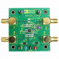
... EVALUATION BOARDS The AD8337evaluation boards provide a family of platforms for testing and evaluating the AD8337 VGA. Three circuit configu- rations are available: • AD8337-EVALZ, dc-coupled, with noninverting gain and dual power supplies • AD8337-EVALZ-INV, dc-coupled, with inverting gain and dual power supplies • ...
Page 24
... INPN PRAO C4 R2 0.1µF 49.9Ω R FB2 R5 100Ω 100Ω R FB1 100Ω DO NOT INSTALL PARTS IN GRAY Figure 80. Schematic—AD8337-EVALZ - Noninverting Configuration GND1 GND GND2 GND3 GND4 RVO1 VOUT 453Ω TP1 1 8 VOUT VPOS U1 RVO3 AD8337 0Ω ...
Page 25
... Not evident in the figures are thermal vias within the pad that solder to the mating pad of the AD8337 chip-scale package. These vias serve as a thermal path and are the primary means of removing heat from the device. The thermal ...
Page 26
... AD8337 Figure 84. Dual-Supply Component Side Copper Figure 85. Dual-Supply Wiring Side Copper Figure 86. Dual-Supply Component Side Silk-Screen Figure 87. Dual-Supply Ground Plane Figure 88. Dual-Supply Power Plane Figure 89. Single-Supply Component Side Copper Figure 90. Single-Supply Wiring Side Copper Figure 91. Single-Supply Component Side Silkscreen Rev Page ...
Page 27
... Panasonic Panasonic Panasonic Panasonic Rev Page AD8337 Mfg. Part Number TP-104-01-02 TP-104-01-00 TP-104-01-06 TP-104-01-07 C0603C104K4RACTU ECJ-1VB2A102K T491A106M010AS AD8337BCPZ-WP 901-143-6RFX BLM18BA750SN1D ERJ-3EKF49R9V ERJ-2GE0R00X ERJ-3EKF1000V ERJ-3EKF4530V Mfg. Part Number TP-104-01-02 TP-104-01-00 TP-104-01-06 TP-104-01-07 C0603C104K4RACTU ECJ-1VB2A102K T491A106M010AS AD8337BCPZ-WP 901-143-6RFX BLM18BA750SN1D ERJ-3EKF49R9V ERJ-2GE0R00X ERJ-3EKF1000V ERJ-3EKF4530V ...
Page 28
... Mfg. Part Number Bisco Industries TP-104-01-02 Nichicon T491A106M010AS Nichicon F921C105MPA KEMET C0603C104K4RACTU Panasonic ECJ-1VB1H223K Panasonic ECJ-1VB2A102K Amphenol 901-143-6RFX Bisco Industries TP-104-01-00 Murata BLM18BA750SN1D Panasonic ERJ-3EKF49R9V Panasonic ERJ-3EKF1002V Panasonic ERJ-3EKF1000V Panasonic ERJ-3EKF4530V Analog Devices, Inc. AD8337BCPZ-WP Analog Devices, Inc. ADR391AUJZ-R2 Analog Devices, Inc. AD8541AR ...
Page 29
... AD8337BCPZ-REEL −40°C to +85°C AD8337BCPZ-REEL7 1 −40°C to +85°C 1 AD8337BCPZ-WP −40°C to +85°C 1 AD8337-EVALZ 1 AD8337-EVALZ-INV 1 AD8337-EVALZ- RoHS Compliant Part. 3.25 0.60 MAX 3.00 SQ 2.75 0.60 MAX 2.95 2.75 SQ TOP VIEW 2.55 0.50 0.40 12° MAX ...
Page 30
... AD8337 NOTES Rev Page ...
Page 31
... NOTES Rev Page AD8337 ...
Page 32
... AD8337 NOTES ©2005–2008 Analog Devices, Inc. All rights reserved. Trademarks and registered trademarks are the property of their respective owners. D05575-0-9/08(C) Rev Page ...