TC1016/17EV Microchip Technology, TC1016/17EV Datasheet - Page 12
TC1016/17EV
Manufacturer Part Number
TC1016/17EV
Description
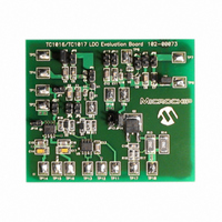
BOARD DEMO FOR TC1016/TC1017
Manufacturer
Microchip Technology
Specifications of TC1016/17EV
Design Resources
TC1016/17EV Gerber Files
Channels Per Ic
1 - Single
Voltage - Output
1.8V, 3V
Current - Output
150mA, 150mA
Voltage - Input
2.7 ~ 6V
Regulator Type
Positive Fixed
Operating Temperature
-40°C ~ 125°C
Board Type
Fully Populated
Utilized Ic / Part
TC1016, TC1017
Processor To Be Evaluated
TC1016 and TC1017
Lead Free Status / RoHS Status
Contains lead / RoHS non-compliant
Lead Free Status / RoHS Status
Lead free / RoHS Compliant, Contains lead / RoHS non-compliant


TC1017
5.0
5.1
Integrated thermal protection circuitry shuts the
regulator off when the die temperature exceeds
approximately 160°C. The regulator remains off until
the die temperature drops to approximately 150°C.
5.2
The TC1017 is available in the SC-70 package. The
thermal resistance for the SC-70 package is
approximately 450°C/W when the copper area used in
the PCB layout is similar to the JEDEC J51-7 high ther-
mal conductivity standard or semi-G42-88 standard.
For applications with a larger or thicker copper area,
the thermal resistance can be lowered. See AN792, “A
Method to Determine How Much Power a SOT-23 Can
Dissipate in an Application”, DS00792, for a method to
determine the thermal resistance for a particular appli-
cation.
The TC1017 power dissipation capability is dependant
upon several variables: input voltage, output voltage,
load current, ambient temperature and maximum
junction temperature. The absolute maximum steady-
state junction temperature is rated at +125°C. The
power dissipation within the device is equal to:
EQUATION 5-1:
The V
compared to the (V
the power dissipation within the LDO to be:
EQUATION 5-2:
To
capability, the following equation is used:
EQUATION 5-3:
DS21813D-page 12
Where:
determine
P
IN
T
T
R
D
J_MAX
A_MAX
THERMAL CONSIDERATIONS
Thermal Shutdown
Power Dissipation: SC-70
JA
x I
=
GND
P
P
V
DMAX
D
IN
= the maximum junction
= the maximum ambient
= the thermal resistance from
the
=
–
term is typically very small when
temperature allowed
temperature
junction to air
IN
V
V
=
OUT
–V
IN
maximum
--------------------------------------------- -
OUT
T
–
J_MAX
V
OUT
) x I
I
LOAD
R
–
LOAD
JA
T
A_MAX
+
I
power
LOAD
V
term, simplifying
IN
I
GND
dissipation
Given the following example:
Find:
1.
2.
3.
In this example, the TC1017 dissipates approximately
158.5 mW and the junction temperature is raised 71°C
over the ambient. The absolute maximum power
dissipation is 155 mW when given a maximum ambient
temperature of 55°C.
Input voltage, output voltage or load current limits can
also be determined by substituting known values in the
power dissipation equations.
Figure 5-1 and Figure 5-2 depict typical maximum
power dissipation versus ambient temperature, as well
as typical maximum current versus ambient tempera-
ture, with a 1V input voltage to output voltage
differential, respectively.
FIGURE 5-1:
Ambient Temperature (SC-70 package).
Internal power dissipation:
Maximum allowable ambient temperature:
Maximum
desired ambient:
P
T
400
350
300
250
200
150
100
DMAX
50
A_MAX
0
-40
I
V
LOAD
OUT
V
T
IN
A
=
=
=
=
=
=
=
-15
allowable
158.5mW
P
=
=
=
=
T
54 C
V
4.1V 2.85
125 C 158.5mW 450 C/W
125 C 71 C
D
J_MAX
IN_MAX
Ambient Temperature (°C)
3.0V to 4.1V
2.85V ±2.5%
120 mA (output current)
55°C (max. desired ambient)
=
=
=
10
Power Dissipation vs.
–
T
----------------------------- -
125 C 55 C
---------------------------------- -
155mW
© 2005 Microchip Technology Inc.
J_MAX
–
–
–
450 C/W
–
R
P
35
power
V
DMAX
JA
OUT_MIN
–
–
0.975
T
60
A
R
dissipation
85
JA
120mA
I
LOAD
110
at
Related parts for TC1016/17EV
Image
Part Number
Description
Manufacturer
Datasheet
Request
R


Part Number:
Description:
IC REG LDO 3.0V 80MA SD SC-70-5
Manufacturer:
Microchip Technology
Datasheet:
Part Number:
Description:
IC REG LDO 3.3V 80MA SD SC70-5
Manufacturer:
Microchip Technology
Datasheet:

Part Number:
Description:
IC REG LDO 2.7V SOT-23-5
Manufacturer:
Microchip Technology
Datasheet:
Part Number:
Description:
IC REG LDO 1.8V 80MA SD SC-70-5
Manufacturer:
Microchip Technology
Datasheet:
Part Number:
Description:
IC REG LDO 1.85V SOT-23-5
Manufacturer:
Microchip Technology
Datasheet:
Part Number:
Description:
IC REG LDO 2.8V SOT-23-5
Manufacturer:
Microchip Technology
Datasheet:
Part Number:
Description:
IC REG LDO 4.0V SOT-23-5
Manufacturer:
Microchip Technology
Datasheet:
Part Number:
Description:
IC REG LDO 4.0V SC70-5
Manufacturer:
Microchip Technology
Datasheet:
Part Number:
Description:
IC CMOS LDO 80MA 3.3V SOT23-5
Manufacturer:
Microchip Technology
Datasheet:
Part Number:
Description:
IC CMOS LDO 80MA 1.8V SOT23-5
Manufacturer:
Microchip Technology
Datasheet:
Part Number:
Description:
IC REG LDO 2.8V 80MA SD SC-70-5
Manufacturer:
Microchip Technology
Datasheet:
Part Number:
Description:
IC REG LDO 2.7V 80MA SD SC-70-5
Manufacturer:
Microchip Technology
Datasheet:

Part Number:
Description:
80mA Tiny CMOS LDO With Shutdown 5 SOT-23 T/R
Manufacturer:
Microchip Technology
Datasheet: