EVALSTSR30-60W STMicroelectronics, EVALSTSR30-60W Datasheet
EVALSTSR30-60W
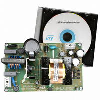
Specifications of EVALSTSR30-60W
EVALSTSR30-60W
Available stocks


Related parts for EVALSTSR30-60W


EVALSTSR30-60W Summary of contents
Page 1
General Features MULTIPOWER BCD TECHNOLOGY ■ LOAD-DEPENDENT CURRENT-MODE CON- ■ TROL: FIXED-FREQUENCY (HEAVY LOAD), FREQUENCY FOLDBACK (LIGHT LOAD), BURST-MODE (NO-LOAD) ON-BOARD HIGH-VOLTAGE START-UP ■ IMPROVED STANDBY FUNCTION ■ LOW QUIESCENT CURRENT (< 2 mA) ■ SLOPE COMPENSATION ■ PULSE-BY-PULSE ...
Page 2
L6668 2 Description L6668 is a current-mode primary controller IC, designed to build single-ended converters. The IC drives the system at fixed frequency at heavy load and an improved Standby function causes a smooth frequency reduction as the load is ...
Page 3
Table 4. Pin Description Pin Pin Name Number 1 HV High-voltage start-up. The pin connected directly to the rectified mains voltage. A 0.8 mA internal current source charges the capacitor connected between pin Vcc and GND to ...
Page 4
L6668 Table 4. Pin Description (continued) Pin Pin Name Number 13 STBY Standby function. This pin is a high-impedance one as long as the voltage on pin COMP is higher than 3V. When the voltage on pin COMP falls below ...
Page 5
Table 5. Electrical Characteristcs (continued 105°C, Vcc=15V, Co=1nF Symbol Parameter REFERENCE VOLTAGE V Output voltage REF V Total variation REF I Short circuit current REF Sink capability in UVLO PWM CONTROL V Maximum level ...
Page 6
L6668 Table 5. Electrical Characteristcs (continued 105°C, Vcc=15V, Co=1nF Symbol Parameter V Low saturation voltage SSsat V High saturation voltage SSclamp SKIPADJ FUNCTION I Input Bias Current bias V Operating range SKIP Hys Hysteresis ...
Page 7
Typical Electrical Performance Figure 5. High-voltage generator ON-state sink current vs (pin 1) HV 1.2 [mA 100 V HV 0.6 0.4 0.2 - (°C) Figure 6. High-voltage generator output (Vcc ...
Page 8
L6668 Figure 11. Start-up & UVLO vs (pin 5) ( OFF while latched off OFF (°C) Figure 12. Vcc Zener voltage vs. Tj Vcc Z ...
Page 9
Figure 17. Oscillator frequency vs. Tj fsw 102 13.3 kΩ 101.5% 101% 100.5% 100% 99.5% Values normalized Tj=25°C, Vcc=15V s w 99% - (°C) Figure 18. ...
Page 10
L6668 Figure 23. Standby thresholds vs (pin 10) COMP 3.6 (V) 3.4 3.2 Disable (voltage rising) 3 Enable (voltage falling) 2.8 2.6 2.4 - (°C) Figure 24. Standby pin dropout vs. Tj Vpin13 - Vpin10 ...
Page 11
Figure 29. S-COMP ramp vs. Tj Vpin15 2.0 (V) Peak 1.5 1.0 0.5 Valley 0.0 - (°C) Figure 30. UVLO saturation vs. Tj Vpin4 1 (V) 0.9 0.8 0.7 0.6 0.5 - (°C) Figure ...
Page 12
L6668 4 Application Information The L6668 is a versatile current-mode PWM controller specific for offline fixed-frequency, peak-current- mode-controlled flyback converters. The device is able to operate in different modes (fig. 34), depending on the converter's load conditions: 1) Fixed frequency ...
Page 13
With reference to the timing diagram of figure 36, when power is first applied to the converter the voltage on the bulk capacitor (Vin) builds up and reaches about 80V, the HV generator is enabled to oper- ate ...
Page 14
L6668 At converter power-down the system will lose regulation as soon as the input voltage is so low that either peak current or maximum duty cycle limitation is tripped. Vcc will then drop and stop IC activity as it falls ...
Page 15
Figure 39. Standby function: frequency shift vs. timing resistors (normalized quantities 0.9 0.9 0.8 0.8 0.7 0 min min 0.6 0 osc osc 0.5 0.5 0.4 0.4 2.5V 2.5V 0.3 0.3 0.2 0.2 0. ...
Page 16
L6668 Figure 40. Load-dependent operating modes: timing diagram COMP 3.0V V(SKIPADJ) f osc OUT Fix. Freq. Mode The operating range of the voltage V(SKIPADJ) is practically limited upwards by the onset of audible noise: typically, with a voltage above 2-2.1V ...
Page 17
Figure 41. Hiccup-mode OCP: timing diagram Vcc Vcc Vcc ON Vcc ON Vcc OFF Vcc OFF 1.5 V 1.5 V OUT OUT OCP latch OCP latch Vcc_OK Vcc_OK A second comparator senses the voltage ...
Page 18
L6668 Figure 43 shows a timing diagram where the PFC_STOP function operation is illustrated under different operating conditions. Figure 42. How the L6668 can switch off a PFC controller at light load L6668 L6668 Figure 43. Operation of PFC_STOP function ...
Page 19
Disable function Latched OTP or OVP functions can be easily realized with the L6668: the IC is equipped with a compara- tor whose non-inverting input is externally available on pin #7 (DIS), and whose inverting input is inter- nally ...
Page 20
L6668 Figure 46. Typical Application: 80W, WRM flyback; Electrical Schematic NTC1 NTC1 F1 T2A250V F1 T2A250V BD1 BD1 DF04M DF04M 264 88 to 264 Vac Vac C1 C1 100 µF 100 µF 400 V 400 V ...
Page 21
... Package information In order to meet environmental requirements, STMicroelectronics offers this device in ECOPACK age. This package has a Lead-free second level interconnect. The category of second level Interconnect is marked on the package and on the inner box label, in compliance with JEDEC Standard JESD97. The maximum ratings related to soldering conditions are also marked on the inner box label. ECOPACK is an STMicroelectronics trademark ...
Page 22
L6668 6 Revision History Table 7. Revision History Date Revision 20-May-2005 15-July-2005 28-July-2005 13-Jan-2006 22/23 1 First Issue. 2 Modify values in Electrical Characteristics 3 Changed the maturity from “Preliminary Data” to “Datasheet”. 4 Absolute Maximum Rating Update (added ESD ...
Page 23
... No license is granted by implication or otherwise under any patent or patent rights of STMicroelectronics. Specifications mentioned in this publication are subject to change without notice. This publication supersedes and replaces all information previously supplied. STMicroelectronics products are not authorized for use as critical components in life support devices or systems without express written approval of STMicroelectronics ...