ADNK-5033-FS27 Avago Technologies US Inc., ADNK-5033-FS27 Datasheet - Page 14
ADNK-5033-FS27
Manufacturer Part Number
ADNK-5033-FS27
Description
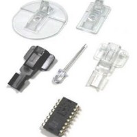
KIT REF DES OPT MOUSE ADNS-5030
Manufacturer
Avago Technologies US Inc.
Datasheets
1.ADNK-5033-FS27.pdf
(24 pages)
2.ADNK-5033-FS27.pdf
(6 pages)
3.ADNK-5033-FS27.pdf
(32 pages)
Specifications of ADNK-5033-FS27
Main Purpose
Reference Design, Optical Mouse
Utilized Ic / Part
ADNS-5030
Wireless Frequency
27 MHz
Interface Type
USB
Modulation
FSK
For Use With/related Products
MC68HC908QY4A, MC68HC908JB12
Lead Free Status / RoHS Status
Lead free / RoHS Compliant
Secondary Attributes
-
Embedded
-
Primary Attributes
-
Lead Free Status / Rohs Status
Lead free / RoHS Compliant


Motion Burst Timing
SCLK
Burst Mode Operation
Burst mode is a special serial port operation mode that
may be used to reduce the serial transaction time for
a motion read. The speed improvement is achieved by
continuous data clocking to or from multiple registers
without the need to specify the register address, and
by not requiring the normal delay period between data
bytes.
Burst mode is activated by reading the Motion_Burst
register. The ADNS-5030 will respond with the contents
of the Delta_X, Delta_Y, SQUAL, Shutter_Upper, Shutter_
Lower, and Maximum_Pixel and Pixel_Sum registers
in that order. The burst transaction can be terminated
anywhere in the sequence after the Delta_X value by
bringing the NCS pin high. After sending the register
address, the micro-controller must wait t
begin reading data. All data bits can be read with no
delay between bytes by driving SCLK at the normal rate.
The data are latched into the output buffer after the last
address bit is received. After the burst transmission is
complete, the micro-controller must raise the NCS line
for at least t
is not available for use until it is reset with NCS, even for
a second burst transmission.
Avago Technologies highly recommends the usage of
burst mode operation in optical mouse sensor design
applications.
14
MOTION_BURST REGISTER ADDRESS
BEXIT
to terminate burst mode. The serial port
FIRST READ OPERATION
READ FIRST BYTE
t
SRAD
SRAD
and then
READ SECOND BYTE
Notes on Power-up and Reset
The ADNS-5030 does not perform an internal power
up self-reset; the NRESET pin must be asserted low
every time power is applied. There are two ways
to reset the chip, either assert low NRESET pin or by
writing 0x5a to register 0x3a. A full reset will thus be
executed. Any register settings must then be reloaded.
During power-up there will be a period of time after the
power supply is high but before any clocks are available.
The table below shows the state of the various pins
during power-up and reset.
State of Signal Pins after VDD is Valid
Pin
NCS
MISO
SCLK
MOSI
XY_LED
Notes on Power Down
The ADNS-5030 can be set in Power Down mode by setting
bit 1 of Register 0x0d. In addition, the SPI port should not
be accessed during power down. (Other ICs on the same
SPI bus can be accessed, as long as the sensor’s NCS
pin is not asserted.) The table below shows the state of
various pins during power down. There are 2 ways to exit
power down, either assert low NRESET pin or by writing
0x5a to Register 0x3a. A full reset will thus be executed.
Wait t
settings must then be reloaded.
* NCS pin must be held to 1 (high) if SPI bus is shared with other devices.
It can be in either state if the sensor is the only device in addition to the
controller microprocessor.
Note: There is long wakeup time from power down. This feature should
not be used for power management during normal mouse motion.
Pin
NRESET
NCS
MISO
SCLK
MOSI
XY_LED
WAKEUP
READ THIRD BYTE
before accessing the SPI port. Any register
During Reset
Ignored
Low
Ignored
Ignored
High
Power Down Active
Undefined
Functional*
Functional*
Low current
Functional
Functional*
After Reset
Functional
Depends on NCS
Depends on NCS
Depends on NCS
Functional
Related parts for ADNK-5033-FS27
Image
Part Number
Description
Manufacturer
Datasheet
Request
R

Part Number:
Description:
KIT REFERENCE DESIGN ADNK-5030
Manufacturer:
Avago Technologies US Inc.
Datasheet:

Part Number:
Description:
A2700 Sample Kit
Manufacturer:
Avago Technologies US Inc.
Datasheet:

Part Number:
Description:
OPTOCOUPLER GATE DRV 2A 16-SOIC
Manufacturer:
Avago Technologies US Inc.
Datasheet:
Part Number:
Description:
OPTOCOUPLER 2CH 2.5A 16-SOIC
Manufacturer:
Avago Technologies US Inc.
Datasheet:

Part Number:
Description:
OPTOCOUPLER GATE DRV 0.4A 16SOIC
Manufacturer:
Avago Technologies US Inc.
Datasheet:

Part Number:
Description:
OPTOCOUPLER 2.0A 250KHZ 8-DIP
Manufacturer:
Avago Technologies US Inc.
Datasheet:

Part Number:
Description:
OPTOCOUPLER 2.0A 250KHZ GW 8-SMD
Manufacturer:
Avago Technologies US Inc.
Datasheet:

Part Number:
Description:
OPTOCOUPLER 2CH 15MBD 3.3V 8SOIC
Manufacturer:
Avago Technologies US Inc.
Datasheet:
Part Number:
Description:
OPTOCOUPLER DARL-OUT 8-DIP
Manufacturer:
Avago Technologies US Inc.
Datasheet:
Part Number:
Description:
OPTOCOUPLER IGBT DRIVE 0.4A 8DIP
Manufacturer:
Avago Technologies US Inc.
Datasheet:
Part Number:
Description:
OPTOCOUPLER DARL-OUT 8-DIP
Manufacturer:
Avago Technologies US Inc.
Datasheet:

Part Number:
Description:
OPTOCOUPLER 1CH 1MBS 8-SMD GW
Manufacturer:
Avago Technologies US Inc.
Datasheet:
Part Number:
Description:
OPTOCOUPLER GATE DRIVER 8-DIP
Manufacturer:
Avago Technologies US Inc.
Datasheet:

Part Number:
Description:
OPTOCOUPLER GATE DRIVER 8-SMD
Manufacturer:
Avago Technologies US Inc.
Datasheet:

Part Number:
Description:
OPTOCOUPLER PHOTOTRANS 4-SMD
Manufacturer:
Avago Technologies US Inc.
Datasheet: