OM6290 NXP Semiconductors, OM6290 Datasheet - Page 34
OM6290
Manufacturer Part Number
OM6290
Description
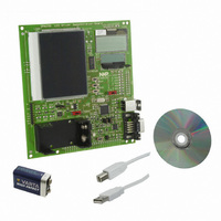
DEMO BOARD LCD GRAPHIC DRIVER
Manufacturer
NXP Semiconductors
Datasheets
1.PCF8576T1118.pdf
(44 pages)
2.OM6290.pdf
(30 pages)
3.OM6290.pdf
(51 pages)
4.OM6290.pdf
(83 pages)
Specifications of OM6290
Main Purpose
Displays, LCD Controller
Embedded
Yes, MCU, 16/32-Bit
Utilized Ic / Part
PCF2119, PCF8531, PCF8576
Primary Attributes
Character, Graphic and Segment LCD Drivers
Secondary Attributes
JTAG, I²C, UART & USB Interfaces
Description/function
Demo Board
Interface Type
USB, I2C, JTAG, UART
Data Bus Width
4 bit, 8 bit, 16 bit
Operating Voltage
1.8 V to 5.5 V
For Use With/related Products
PCF8576DT, PCF2119S, PCF8531
Lead Free Status / RoHS Status
Lead free / RoHS Compliant
Lead Free Status / RoHS Status
Lead free / RoHS Compliant, Lead free / RoHS Compliant
Other names
568-4703


NXP Semiconductors
PCF2119X
Product data sheet
10.2.2.5 Curs_disp_shift
Bit D: The display is on when bit D = 1 and off when bit D = 0. Display data in the DDRAM
is not affected and can be displayed immediately by setting bit D = 1.
When the display is off (bit D = 0) the chip is in partial power-down mode:
Three oscillator cycles are required after sending the ‘display off’ instruction to ensure all
outputs are at V
during partial power-down mode (‘display off’) the chip can still execute instructions. Even
lower current consumption is obtained by inhibiting the oscillator (pin OSC to V
To ensure I
Recovery from power-down mode:
Bit C: The cursor is displayed when bit C = 1 and inhibited when bit C = 0. Even if the
cursor disappears, bit I_D and bit S (see
display data write. The cursor is displayed using 5 dots in the 8th line (see
Bit B: The character indicated by the cursor blinks when bit B = 1. The character blink is
displayed by switching between display characters and all dots on with a period of
approximately 1 second, with
Table 20.
Bit
RS
R/W
7 to 4
3
2
1 to 0
•
•
•
•
•
•
•
•
The LCD outputs are connected to V
The V
the parallel bus ports DB7 to DB0 should be connected to V
pins RS and R/W should be connected to V
pin PD should be connected to V
pin PD should be connected back to V
if necessary pin OSC should be connected back to V
a Display_ctl instruction with bit D = 1 should be sent
Symbol
-
-
-
SC
RL
-
LCD
Curs_disp_shift bit description
DD
generator and bias generator are turned off
< 1 μA:
All information provided in this document is subject to legal disclaimers.
SS
, afterwards the oscillator can be stopped. If the oscillator is running
Value
0
0
0001
0
1
0
1
00
Rev. 9 — 14 April 2011
f
blink
DD
=
-------------- -
52224
SS
Section
f
Description
see
fixed value
cursor move or display shift
shift or move to the right or left
fixed value
osc
SS
move cursor
shift display
left shift or move
right shift or move
Table 10
DD
10.2.2.3) remain in operation during
or left open-circuit
DD
DD
LCD controllers/drivers
PCF2119x
© NXP B.V. 2011. All rights reserved.
Figure
SS
).
17).
34 of 83
Related parts for OM6290
Image
Part Number
Description
Manufacturer
Datasheet
Request
R

Part Number:
Description:
NXP Semiconductors designed the LPC2420/2460 microcontroller around a 16-bit/32-bitARM7TDMI-S CPU core with real-time debug interfaces that include both JTAG andembedded trace
Manufacturer:
NXP Semiconductors
Datasheet:

Part Number:
Description:
NXP Semiconductors designed the LPC2458 microcontroller around a 16-bit/32-bitARM7TDMI-S CPU core with real-time debug interfaces that include both JTAG andembedded trace
Manufacturer:
NXP Semiconductors
Datasheet:
Part Number:
Description:
NXP Semiconductors designed the LPC2468 microcontroller around a 16-bit/32-bitARM7TDMI-S CPU core with real-time debug interfaces that include both JTAG andembedded trace
Manufacturer:
NXP Semiconductors
Datasheet:
Part Number:
Description:
NXP Semiconductors designed the LPC2470 microcontroller, powered by theARM7TDMI-S core, to be a highly integrated microcontroller for a wide range ofapplications that require advanced communications and high quality graphic displays
Manufacturer:
NXP Semiconductors
Datasheet:
Part Number:
Description:
NXP Semiconductors designed the LPC2478 microcontroller, powered by theARM7TDMI-S core, to be a highly integrated microcontroller for a wide range ofapplications that require advanced communications and high quality graphic displays
Manufacturer:
NXP Semiconductors
Datasheet:
Part Number:
Description:
The Philips Semiconductors XA (eXtended Architecture) family of 16-bit single-chip microcontrollers is powerful enough to easily handle the requirements of high performance embedded applications, yet inexpensive enough to compete in the market for hi
Manufacturer:
NXP Semiconductors
Datasheet:
Part Number:
Description:
The XA-S3 device is a member of Philips Semiconductors? XA(eXtended Architecture) family of high performance 16-bitsingle-chip microcontrollers
Manufacturer:
NXP Semiconductors
Datasheet:

Part Number:
Description:
The NXP BlueStreak LH75401/LH75411 family consists of two low-cost 16/32-bit System-on-Chip (SoC) devices
Manufacturer:
NXP Semiconductors
Datasheet:
Part Number:
Description:
The NXP LPC3130/3131 combine an 180 MHz ARM926EJ-S CPU core, high-speed USB2
Manufacturer:
NXP Semiconductors
Datasheet:
Part Number:
Description:
The NXP LPC3141 combine a 270 MHz ARM926EJ-S CPU core, High-speed USB 2
Manufacturer:
NXP Semiconductors
Part Number:
Description:
The NXP LPC3143 combine a 270 MHz ARM926EJ-S CPU core, High-speed USB 2
Manufacturer:
NXP Semiconductors

Part Number:
Description:
The NXP LPC3152 combines an 180 MHz ARM926EJ-S CPU core, High-speed USB 2
Manufacturer:
NXP Semiconductors
Part Number:
Description:
The NXP LPC3154 combines an 180 MHz ARM926EJ-S CPU core, High-speed USB 2
Manufacturer:
NXP Semiconductors

Part Number:
Description:
Standard level N-channel enhancement mode Field-Effect Transistor (FET) in a plastic package using NXP High-Performance Automotive (HPA) TrenchMOS technology
Manufacturer:
NXP Semiconductors
Datasheet: