C8051T606ZDB Silicon Laboratories Inc, C8051T606ZDB Datasheet - Page 4
C8051T606ZDB
Manufacturer Part Number
C8051T606ZDB
Description
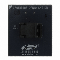
CARD DAUGHTER QFN10 SOCKET
Manufacturer
Silicon Laboratories Inc
Datasheets
1.C8051T600EDB.pdf
(188 pages)
2.C8051T606TDB.pdf
(1 pages)
3.C8051T606TDB.pdf
(14 pages)
Specifications of C8051T606ZDB
Module/board Type
Socket Module - QFN
Maximum Operating Temperature
+ 85 C
Minimum Operating Temperature
- 40 C
Lead Free Status / RoHS Status
Lead free / RoHS Compliant
For Use With/related Products
C8051T606
Lead Free Status / Rohs Status
Lead free / RoHS Compliant
Other names
336-1668


C8051T606-DK
6. Example Source Code
Example source code and register definition files are provided in the “SiLabs\MCU\Examples\C8051T60x”
directory during IDE installation. These files may be used as a template for code development. The comments in
each example file indicate which development tool chains were used when testing the.
6.1. Register Definition Files
Register definition files C8051T600.inc, C8051T600_defs.h and compiler_defs.h define all SFR registers and bit-
addressable control/status bits. They are installed into the “SiLabs\MCU\Examples\C8051T60x” directory during
IDE installation. The register and bit names are identical to those used in the C8051T60x datasheet.
7. Development Boards
The C8051T606 Development Kit includes a main board which interfaces to various daughter boards. The
“C8051T600 Emulation Daughter Board” contains a C8051F300 device to be used for preliminary software
development. The socketed C8051T606 daughter boards allow programming and evaluation of the actual
C8051T606 devices. Numerous input/output (I/O) connections are provided on the main board to facilitate
prototyping. Refer to Figure 2 for the locations of the various connectors on the main board. Figure 3, Figure 4 and
Figure 5 show the available daughter boards that can be used with the C8051T606 main board.
4
5. Save the project when finished with the debug session to preserve the current target build configuration,
editor settings and the location of all open debug views. To save the project, select Project
As... from the menu. Create a new name for the project and click on Save.
P1, P2
P3
J1
J2
J3
J8
J10
Daughter board connection (Daughter boards are plugged into the P1 and P2 connectors for
evaluation and programming)
Power connector (accepts input from 7.5 to 15 VDC unregulated power adapter)
USB Debug connector
RS-232 connector
LED/Switch/RS-232 connection block
Direct device pin connection block
VPP supply connection (used when programming EPROM devices)
Rev. 0.1
Save Project
Related parts for C8051T606ZDB
Image
Part Number
Description
Manufacturer
Datasheet
Request
R

Part Number:
Description:
SMD/C°/SINGLE-ENDED OUTPUT SILICON OSCILLATOR
Manufacturer:
Silicon Laboratories Inc
Part Number:
Description:
Manufacturer:
Silicon Laboratories Inc
Datasheet:
Part Number:
Description:
N/A N/A/SI4010 AES KEYFOB DEMO WITH LCD RX
Manufacturer:
Silicon Laboratories Inc
Datasheet:
Part Number:
Description:
N/A N/A/SI4010 SIMPLIFIED KEY FOB DEMO WITH LED RX
Manufacturer:
Silicon Laboratories Inc
Datasheet:
Part Number:
Description:
N/A/-40 TO 85 OC/EZLINK MODULE; F930/4432 HIGH BAND (REV E/B1)
Manufacturer:
Silicon Laboratories Inc
Part Number:
Description:
EZLink Module; F930/4432 Low Band (rev e/B1)
Manufacturer:
Silicon Laboratories Inc
Part Number:
Description:
I°/4460 10 DBM RADIO TEST CARD 434 MHZ
Manufacturer:
Silicon Laboratories Inc
Part Number:
Description:
I°/4461 14 DBM RADIO TEST CARD 868 MHZ
Manufacturer:
Silicon Laboratories Inc
Part Number:
Description:
I°/4463 20 DBM RFSWITCH RADIO TEST CARD 460 MHZ
Manufacturer:
Silicon Laboratories Inc
Part Number:
Description:
I°/4463 20 DBM RADIO TEST CARD 868 MHZ
Manufacturer:
Silicon Laboratories Inc
Part Number:
Description:
I°/4463 27 DBM RADIO TEST CARD 868 MHZ
Manufacturer:
Silicon Laboratories Inc
Part Number:
Description:
I°/4463 SKYWORKS 30 DBM RADIO TEST CARD 915 MHZ
Manufacturer:
Silicon Laboratories Inc
Part Number:
Description:
N/A N/A/-40 TO 85 OC/4463 RFMD 30 DBM RADIO TEST CARD 915 MHZ
Manufacturer:
Silicon Laboratories Inc
Part Number:
Description:
I°/4463 20 DBM RADIO TEST CARD 169 MHZ
Manufacturer:
Silicon Laboratories Inc