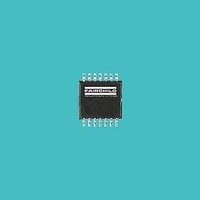
FAN5232MTCX Fairchild Semiconductor, FAN5232MTCX Datasheet - Page 2

FAN5232MTCX
Manufacturer Part Number
FAN5232MTCX
Description
IC CTRLR PWM BUCK ADJ 14TSSOP
Manufacturer
Fairchild Semiconductor
Datasheet
1.FAN5232MTC.pdf
(9 pages)
Specifications of FAN5232MTCX
Applications
Controller, LCD
Voltage - Input
5.6 ~ 24 V
Number Of Outputs
3
Voltage - Output
3.3V, 5V, Adjustable
Operating Temperature
-20°C ~ 85°C
Mounting Type
Surface Mount
Package / Case
14-TSSOP
Output Voltage
5 V to 16 V
Input Voltage
5.6 V to 24 V
Switching Frequency
300 KHz
Operating Temperature Range
- 20 C to + 85 C
Mounting Style
SMD/SMT
Duty Cycle (max)
80 %
Isolated/non-isolated
Non Isolated
Lead Free Status / RoHS Status
Lead free / RoHS Compliant
Available stocks
Company
Part Number
Manufacturer
Quantity
Price
Part Number:
FAN5232MTCX
Manufacturer:
FAIRCHILD/仙童
Quantity:
20 000
FAN5232
Pin Assignments
Pin Description
Absolute Maximum Ratings
Note:
1. Functional operation under any of these conditions is NOT implied. Performance and reliability are guaranteed only if
2
VBATT Pin
PHASE, IFB, SDWN Pins
CPUMP, HSD Pins
All Other Pins
Thermal Resistance,
Junction Temperature
Storage Temperature
Lead Temperature, Soldering 10 sec.
Pin Number
Operating Conditions are not exceeded.
10
11
12
13
14
1
2
3
4
5
6
7
8
9
Parameter
3V_ALWAYS
5V_ALWAYS
Pin Name
SDNADJ
PWRGD
VFBSW
CPUMP
VBATT
SDWN
AGND
PGND
ISNS
HSD
LSD
SW
J-A
J-C
5V_ALWAYS
3V_ALWAYS
Battery Voltage. Battery voltage sensor.
3.3V-ALWAYS Linear Regulator. Total load current on pins 2 and 3 together
must not exceed 50mA.
5V-ALWAYS Linear Regulator. Total load current on pins 2 and 3 together
must not exceed 50mA.
Analog Ground.
IC Shutdown. Puts entire chip into shutdown. OFF=0. ON=1.
Shutdown and Softstart for the Switcher. OFF=0. ON=1.
Switcher Output OK. An open collector output that will be low if the switcher
output is out of spec.
Voltage Feedback for the Switcher.
Ground for the Switcher. Connect by the shortest possible path to the source
of the low side MOSFET.
Low Side FET Driver for the Switcher. Connect this pin through a resistor to
the gate of an N-channel MOSFET.
High Side FET Source and Low Side FET Drain Switching Node.
Current Feedback for the Switcher. Connect by the shortest possible path to
a resistor connected to the drain of the low side MOSFET.
High Side FET Driver for the Switcher. Connect this pin through a resistor to
the gate of an N-channel MOSFET.
Charge Pump for the Switcher. Generates gate drive voltage for the high-side
MOSFET.
SDNADJ
PWRGD
VBATT
SDWN
AGND
1
Conditions
1
2
3
4
5
6
7
Pin Function Description
Min.
-0.3
-0.3
-0.3
-65
-5
14
13
12
11
10
9
8
CPUMP
HSD
ISNS
SW
LSD
PGND
VFB
Typ.
100
32
Max.
PRODUCT SPECIFICATION
150
150
300
6.5
29
29
34
REV. 1.1.1 10/7/02
Units
°C/W
°C/W
°C
°C
°C
V
V
V
V


