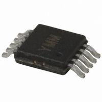
MIC2169BMM Micrel Inc, MIC2169BMM Datasheet - Page 11

MIC2169BMM
Manufacturer Part Number
MIC2169BMM
Description
IC CTRLR PWM SYNC BUCK 10-MSOP
Manufacturer
Micrel Inc
Datasheet
1.MIC2169YMM.pdf
(15 pages)
Specifications of MIC2169BMM
Pwm Type
Voltage Mode
Number Of Outputs
1
Frequency - Max
550kHz
Duty Cycle
92%
Voltage - Supply
3 V ~ 14.5 V
Buck
Yes
Boost
No
Flyback
No
Inverting
No
Doubler
No
Divider
No
Cuk
No
Isolated
No
Operating Temperature
-40°C ~ 85°C
Package / Case
10-MSOP, Micro10™, 10-uMAX, 10-uSOP
Frequency-max
550kHz
Lead Free Status / RoHS Status
Contains lead / RoHS non-compliant
Available stocks
Company
Part Number
Manufacturer
Quantity
Price
Company:
Part Number:
MIC2169BMM
Manufacturer:
MOSTEK
Quantity:
6 235
Part Number:
MIC2169BMM
Manufacturer:
MICREL/麦瑞
Quantity:
20 000
Part Number:
MIC2169BMMTR
Manufacturer:
MICROCHIP/微芯
Quantity:
20 000
It can be seen from the transfer function G(s) and the gain
curve that the output inductor and capacitor create a two pole
system with a break frequency at:
Therefore, f
By looking at the phase curve, it can be seen that the output
capacitor ESR (0.025Ω) cancels one of the two poles (LC
system by introducing a zero at:
Therefore, F
From the point of view of compensating the voltage loop, it
is recommended to use higher ESR output capacitors since
they provide a 90° phase gain in the power path. For com-
parison purposes, Figure 6 shows the same phase curve
with an ESR value of 0.002Ω.
It can be seen from Figure 5 that at 50kHz, the phase is
approximately –90° versus Figure 6 where the number is
–150°. This means that the transconductance error ampli-
fi er has to provide a phase boost of about 45° to achieve a
closed-loop phase margin of 45° at a crossover frequency
of 50kHz for Figure 4, versus 105° for Figure 6. The simple
RC and C2 compensation scheme allows a maximum error
amplifi er phase boost of about 90°. Therefore, it is easier to
stabilize the MIC2169 voltage control loop by using high ESR
value output capacitors.
March 2009
Figure 6. The Phase Curve with ESR = 0.002Ω
f
ZERO
80
0
80
50
00
50
0
50
00
50
0
0
f
LC
00
LC
00
00
00
ZERO
Figure 5. Phase Curve for G(s)
=
=
= 3.6kHz
2
2
× ×
×
= 6.36kHz.
π
π
. 0
. 0
3
ESR C
L C
3
1
×
1
×
OUT
. 0
OUT
. 0
f
f
4
4
. 0
. 0
5
5
000000
000000
. 0
. 0
6
6
OUT
)
11
g
It is undesirable to have high error amplifi er gain at high
frequencies because high frequency noise spikes would be
picked up and transmitted at large amplitude to the output,
thus, gain should be permitted to fall off at high frequencies. At
low frequency, it is desireable to have high open-loop gain to
attenuate the power line ripple. Thus, the error amplifi er gain
should be allowed to increase rapidly at low frequencies.
The transfer function with R1, C1, and C2 for the internal
g
equation:
The above equation can be simplified by assuming
C2<<C1,
From the above transfer function, one can see that R1 and
C1 introduce a zero and R1 and C2 a pole at the following
frequencies:
Figures 7 and 8 show the gain and phase curves for the above
transfer function with R1 = 9.3k, C1 = 1000pF, C2 = 100pF,
and g
amplifi er exhibits approximately 45° of phase margin.
m
m
Error Amplifier(z)
Error Amplifier(z)
Error Amplifi er
error amplifi er can be approximated by the following
Fzero=
Fpole =
Fpole@origin =
m
.00
60
= .005Ω
60
40
20
Figure 7. Error Amplifi er Gain Curve
. 0
000
3
1
1
/
/
2
2
–1
π × R1 × C1
π × C2 × R1
. It can be seen that at 50kHz, the error
=
. 0
=
g
4
1
m
g
/
m
2
×
π × C1
×
⎡
⎢
⎢
⎢
⎢
⎣
s
⎡
⎢
⎣
s
×
. 0
×
(
f
C1 C2 1 R1
5
( )
C1 1 R1 C2 S
1 R 1 S C1
+
+
(
1 R 1 S C1
+
+
. 0
)
⎛
⎜
⎝
× ×
6
+
× ×
×
0000000
×
. 0
C1 C2 S
×
M9999-032409
7
C1 C2
×
)
⎤
⎥
⎦
+
×
⎞
⎟
⎠
⎤
⎥
⎥
⎥
⎥
⎦


