LM5000SDX-6/NOPB National Semiconductor, LM5000SDX-6/NOPB Datasheet - Page 4
LM5000SDX-6/NOPB
Manufacturer Part Number
LM5000SDX-6/NOPB
Description
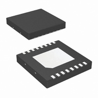
IC REG SWITCHING HI VOLT 16-LLP
Manufacturer
National Semiconductor
Type
Step-Up (Boost), Flyback, Forward Converter, PWM - Current Moder
Datasheet
1.LM5000SD-3NOPB.pdf
(18 pages)
Specifications of LM5000SDX-6/NOPB
Internal Switch(s)
Yes
Synchronous Rectifier
No
Number Of Outputs
1
Voltage - Output
Adjustable
Current - Output
2A
Frequency - Switching
600kHz, 1.3MHz
Voltage - Input
3.1 ~ 40 V
Operating Temperature
-40°C ~ 125°C
Mounting Type
*
Package / Case
16-LLP
Voltage - Supply
3.1 V ~ 40 V
Frequency-max
1.55MHz
Duty Cycle
90%
Pwm Type
Current Mode
Buck
No
Boost
Yes
Flyback
Yes
Inverting
No
Doubler
No
Divider
No
Cuk
No
Isolated
No
For Use With
LM5000EVAL - EVALUATION BOARD FOR LM5000
Lead Free Status / RoHS Status
Lead free / RoHS Compliant
Other names
LM5000SDX-6


www.national.com
θ
JA
Note 1: Absolute maximum ratings are limits beyond which damage to the device may occur. Operating Ratings are conditions for which the device is intended
to be functional, but device parameter specifications may not be guaranteed. For guaranteed specifications and test conditions, see the Electrical Characteristics.
Note 2: The maximum allowable power dissipation is a function of the maximum junction temperature, T
θ
dissipation at any ambient temperature is calculated using: P
excessive die temperature, and the regulator will go into thermal shutdown.
Note 3: The human body model is a 100 pF capacitor discharged through a 1.5kΩ resistor into each pin. The machine model is a 200pF capacitor discharged
directly into each pin.
Note 4: All limits guaranteed at room temperature (standard typeface) and at temperature extremes (bold typeface). All room temperature limits are 100%
production tested. All limits at temperature extremes are guaranteed via correlation using standard Statistical Quality Control (SQC) methods. All limits are used
to calculate Average Outgoing Quality Level (AOQL).
Note 5: Typical numbers are at 25°C and represent the most likely norm.
Note 6: Bias current flows into FB pin.
Note 7: Supply voltage, bias current product will result in aditional device power dissipation. This power may be significant. The thermal dissipation design should
take this into account.
Symbol
JA
, and the ambient temperature, T
Thermal Resistance
Parameter
A
. See the Electrical Characteristics table for the thermal resistance of various layouts. The maximum allowable power
TSSOP, Package only
LLP, Package only
D
(MAX) = (T
Conditions
J(MAX)
4
− T
A
)/θ
JA
. Exceeding the maximum allowable power dissipation will cause
(Note 4)
Min
J
(MAX), the junction-to-ambient thermal resistance,
(Note 5)
Typ
150
45
(Note 4)
Max
Units
°C/W
Related parts for LM5000SDX-6/NOPB
Image
Part Number
Description
Manufacturer
Datasheet
Request
R

Part Number:
Description:
IC REG SWITCHING HI VOLT 16-LLP
Manufacturer:
National Semiconductor
Datasheet:

Part Number:
Description:
IC,SMPS CONTROLLER,CURRENT-MODE,LLCC,16PIN,PLASTIC
Manufacturer:
National Semiconductor

Part Number:
Description:
High Voltage Switch Mode Regulator
Manufacturer:
National Semiconductor Corporation
Datasheet:
Part Number:
Description:
Enhanced Plastic High Voltage Switch Mode Regulator
Manufacturer:
National Semiconductor Corporation
Datasheet:
Part Number:
Description:
National Semiconductor [8-Bit D/A Converter]
Manufacturer:
National Semiconductor
Datasheet:
Part Number:
Description:
National Semiconductor [Media Coprocessor]
Manufacturer:
National Semiconductor
Datasheet:
Part Number:
Description:
Digitally Controlled Tone and Volume Circuit with Stereo Audio Power Amplifier, Microphone Preamp Stage and National 3D Sound
Manufacturer:
National Semiconductor
Datasheet:
Part Number:
Description:
Digitally Controlled Tone and Volume Circuit with Stereo Audio Power Amplifier, Microphone Preamp Stage and National 3D Sound
Manufacturer:
National Semiconductor
Datasheet:
Part Number:
Description:
AC97 Rev 2 Codec with Sample Rate Conversion and National 3D Sound
Manufacturer:
National Semiconductor
Part Number:
Description:
Manufacturer:
National Semiconductor
Datasheet:
Part Number:
Description:
Manufacturer:
National Semiconductor
Datasheet:
Part Number:
Description:
General Purpose, Low Voltage, Low Power, Rail-to-Rail Output Operational Amplifiers
Manufacturer:
National Semiconductor
Datasheet:
Part Number:
Description:
8-bit 20 MSPS flash A/D converter.
Manufacturer:
National Semiconductor
Datasheet:
Part Number:
Description:
Low Noise Quad Operational Amplifier
Manufacturer:
National Semiconductor
Datasheet: