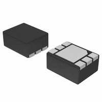
NCP349MNAETBG ON Semiconductor, NCP349MNAETBG Datasheet

NCP349MNAETBG
Specifications of NCP349MNAETBG
Available stocks
Related parts for NCP349MNAETBG
NCP349MNAETBG Summary of contents
Page 1
NCP349 Positive Overvoltage Protection Controller with Internal Low R ON The NCP349 is able to disconnect the systems from its output pin when wrong input operating conditions are detected. The system is positive overvoltage protected up to +28 V. This ...
Page 2
Wall Adapter − AC/DC − USB ENABLE/ Microprocessor Figure 1. Typical Application Circuit 7 INPUT 1 EN Block EN 6 Figure 2. Functional Block Diagram NCP349 CC/CV OUT 5 Charger or 4 ...
Page 3
PIN FUNCTION DESCRIPTION Pin No. Symbol Function INPUT Input Voltage Pins. These pins are connected to the Wall Adapoter (AC−DC, Vbus ..). low ESR ceramic capacitor, or larger, must be connected between these pins ...
Page 4
... Disable Time NOTE: Electrical parameters are guaranteed by correlation across the full range of temperature. 4. Additional UVLO and OVLO thresholds ranging from UVLO and from OVLO can be manufactured. Contact your ON Semiconductor representative for availability. (Min/Max limits values (−40°C < T < +85°C) and V ...
Page 5
UVLO 0.3 V out t start 1.2 V FLAG Figure 3. Startup 1 dis out V − DS(on) 0.3 V FLAG Figure 5. Disable ...
Page 6
TYPICAL OPERATING CHARACTERISTICS Figure 7. Startup V = Ch1 Ch3 in out Figure 9. FLAG Going Up Delay V = Ch3, FLAG = Ch2 out Figure 11. Initial Overvoltage Delay V = Ch1 Ch2, FLAG = ...
Page 7
TYPICAL OPERATING CHARACTERISTICS Figure 13. Inrush Current with C I charge = 1 A, Output Wall Adaptor Inductance 1 mH Figure 15. Output Short Circuit (Zoom Fig. 14) = 100 mF, out http://onsemi.com 7 Figure 14. Output Short Circuit ...
Page 8
IN IN Operation The NCP349 provides overvoltage protection for positive voltage low R protects the systems (i.e.: charger) connected on the Vout pin, against positive overvoltage. At powerup, with EN pin = low, the output ...
Page 9
out FLAG = Low Reset Timer V < UVLO > OVLO out FLAG = Low Timer Count OVLO > V > UVLO in Timer Check Reset Timer V < UVLO ...
Page 10
Undervoltage Lockout (UVLO) To ensure proper operation under any conditions, the device has a built−in undervoltage lockout (UVLO) circuit. During V positive going slope, the output remains in disconnected from input until V voltage is below UVLO, in plus hysteresis, ...
Page 11
... ORDERING INFORMATION Device NCP349MNTBG NCP349MNAETBG NCP349MNBGTBG NCP349MNBKTBG †For information on tape and reel specifications, including part orientation and tape sizes, please refer to our Tape and Reel Packaging Specifications Brochure, BRD8011/D. SELECTION GUIDE The NCP349 can be available in several undervoltage and overvoltage thresholds versions. Part number is designated as follows: ...
Page 12
... B NOTE 3 0.05 C *For additional information on our Pb−Free strategy and soldering details, please download the ON Semiconductor Soldering and Mounting Techniques Reference Manual, SOLDERRM/D. N. American Technical Support: 800−282−9855 Toll Free USA/Canada Europe, Middle East and Africa Technical Support: Phone: 421 33 790 2910 Japan Customer Focus Center Phone: 81− ...


