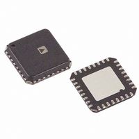
ADN8831ACPZ-REEL7 Analog Devices Inc, ADN8831ACPZ-REEL7 Datasheet - Page 14

ADN8831ACPZ-REEL7
Manufacturer Part Number
ADN8831ACPZ-REEL7
Description
IC THERMO COOLER CTRLR 32LFCSP
Manufacturer
Analog Devices Inc
Datasheet
1.ADN8831ACPZ-REEL7.pdf
(20 pages)
Specifications of ADN8831ACPZ-REEL7
Applications
Thermoelectric Cooler
Current - Supply
8mA
Voltage - Supply
3 V ~ 5.5 V
Operating Temperature
-40°C ~ 85°C
Mounting Type
Surface Mount
Package / Case
32-LFCSP
Ic Function
Thermoelectric Cooler Controller
Supply Voltage Range
3V To 5.5V
Operating Temperature Range
-40°C To +85°C
Digital Ic Case Style
LFCSP
No. Of Pins
32
Msl
MSL 1 - Unlimited
Lead Free Status / RoHS Status
Lead free / RoHS Compliant
Other names
ADN8831ACPZ-REEL7TR
Available stocks
Company
Part Number
Manufacturer
Quantity
Price
Part Number:
ADN8831ACPZ-REEL7
Manufacturer:
ADI/亚德诺
Quantity:
20 000
ADN8831
APPLICATIONS
SIGNAL FLOW
The ADN8831 integrates two auto-zero amplifiers defined as
the Chop1 amplifier and Chop2 amplifier. Both of the
amplifiers can be used as standalone amplifiers, thus, the
implementation of temperature control can vary.
shows the signal flow through the ADN8831, and a typical
implementation of the temperature control loop using the
Chop1 and Chop2 amplifiers.
In
the thermistor input amplifier and the PID compensation
amplifier, respectively. The thermistor input amplifier gains the
thermistor voltage then outputs to the PID compensation
amplifier. The PID compensation amplifier then compensates a
loop response over the frequency domain.
The output from the compensation loop at OUT2 is fed to the
linear MOSFET gate driver. The voltage at LFB is fed with
OUT2 into the PWM MOSFET gate driver. Including the
external transistors, the gain of the differential output section is
fixed at 5. For details on the output drivers, see the
Driver Amplifier
THERMISTOR SETUP
The thermistor has a nonlinear relationship to temperature;
near optimal linearity over a specified temperature range can be
achieved with the proper value of R
thermistor. First, the resistance of the thermistor must be
known, where
Figure 17
17.68kΩ
7.68kΩ
V
, the Chop1 and Chop2 amplifiers are configured as
REF
R
R
R
(10kΩ @ 25°C)
X
TH
section.
V
REF
/2
2
THERMISTOR INPUT
AMPLIFIER
A
V
= R
3
FB
IN1P
IN1N
/(R
R
TH
FB
CHOP1
X
+
–
+ R
placed in series with the
C
) – R
OUT1
FB
V
/R
OUT1
4
Figure 17
V
TEMPSET
MOSFET
Figure 17. Signal Flow Block Diagram
Z
1
5
PID COMPENSATOR
AMPLIFIER
A
Rev. 0 | Page 14 of 20
V
= Z
6
IN2P
IN2N
2
/Z
1
+
CHOP2
–
Z
2
T
T
thermistor data sheets. In some cases, only the B constant is
given, R
Where, R
R
THERMISTOR AMPLIFIER (CHOP1)
The Chop1 amplifier can be used as a thermistor input
amplifier. In
thermistor temperature. The voltage at OUT1 is expressed as
Where, R
calculated as
LOW
MID
X
is then found as
OUT2
is the average. These resistances can be found in most
V
and T
R
R
R
R
R
R
V
OUT
TH
LOW
MID
HIGH
X
OUT2
=
TH
7
TH
=
TH
R
=
1
is calculated as
HIGH
MOSFET DRIVER
A
=
⎛
⎜
⎜
⎝
X
is a resistance at T[K], R
is a thermistor, R
=
=
CONTROL
V
R
=
R
Figure 17, the output voltage is a function of the
R
+
= 5
R
⎛
⎜ ⎜
⎝
R
LOW
R
TH
are the endpoints of the temperature range and
TH
R
R
exp
TH
TH
TH
@
@
R
R
@
⎧
⎪
⎨
⎪ ⎩
@
FB
T
MID
+
B
T
MID
T
R
25
⎛
⎜ ⎜
⎝
LOW
R
LINEAR
PWM
HIGH
LOW
T
°
1
X
C
+
−
−
R
T
MID
+
R
1
X
R
R
SPGATE
SNGATE
LNGATE
R
FB
is a compensation resistor. R is
LPGATE
⎞
⎟ ⎟
⎠
R
HIGH
⎫
⎪
⎬
⎪ ⎭
HIGH
SFB
LFB
+
1
R
⎞
⎟ ⎟
⎠
is a resistance at T
−
×
−
2
V
R
2
REF
2
R
MID
LOW
LPF
R
HIGH
TEC
R
⎞
⎟
⎟
⎠
[K].


