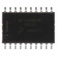
MC14489BDWE Freescale Semiconductor, MC14489BDWE Datasheet

MC14489BDWE
Specifications of MC14489BDWE
Available stocks
Related parts for MC14489BDWE
MC14489BDWE Summary of contents
Page 1
MOTOROLA SEMICONDUCTOR TECHNICAL M u Iti-Character lED Display/lamp CMOS The MC144898 is a flexible light-emitting-diode terfaces to individual lamps, 7-segment both. LEOs wired with common cathodes are driven in a multiplexed-by-5 fashion. Communication with an MCUIMPU is established through a ...
Page 2
DATA IN 11 CLOCK 10 ENABLE BitGrabber CONFIGURATION REGISTER 8 BITS OSCILLATOR AND POR CONTROL LOGIC 5 BANK SWITCHES (FETs BANK 1 BANK 2 BANK 3 BANK 4 BANK 5 MAXIMUM RATINGS* (Voltages Referenced ...
Page 3
ELECTRICAL CHARACTERISTICS (Voltages Referenced – 130 C* unless otherwise indicated) Symbol Parameter V DD Power Supply Voltage Range of LED Drive Circuitry V DD (stby) Minimum Standby Voltage V IL Maximum ...
Page 4
AC ELECTRICAL CHARACTERISTICS Symbol f clk Serial Data Clock Frequency, Single Device or Cascaded Devices NOTE: Refer to Clock t w below (Figure 1) t PLH , Maximum Propagation Delay, Clock to Data Out t PHL (Figures 1 and 5) ...
Page 5
CLOCK 50% 10 1/f clk t PLH t PHL 90% DATA OUT 50% 10% t TLH t THL Figure 1. VALID 50% DATA 50% CLOCK Figure ...
Page 6
PIN DESCRIPTIONS DIGITAL INTERFACE Data In (Pin 12) Serial Data Input. The bit stream begins with the MSB and is shifted in on the low–to–high transition of Clock. When the device is not cascaded, the bit pattern is either 1 ...
Page 7
Anode–Driver Current Sources. These outputs are close- ly–matched current sources which directly tie to the anodes of external discrete LEDs (lamps) or display segment LEDs. Each output is capable ...
Page 8
Table 1. Triple-Mode Segment Decoder Function Table Bank Nibble Value Binary Hexadecimal MSB $ ...
Page 9
Ç Ç Ç Ç Ç Ç Ç Ç Ç Ç Ç Ç Ç Ç Ç Ç Ç Ç Ç Ç Ç Ç Ç Ç Ç Ç Ç Ç Ç Ç Ç Ç Ç Ç Ç Ç Ç Ç Ç Ç ...
Page 10
OPTIONAL DATA OUT CMOS DATA IN MCU/MPU CLOCK ENABLE Figure 9. Non–Cascaded Application Example: 5 Character Common Cathode LED Display with Two Intensities as Controlled via Serial Port ...
Page 11
II) ~o~ z~z <~< < > Lt ~ :§: Figure 10. Bit Stream Formats ...
Page 12
Figure 11. Bit Stream Formats for Three Devices Cascaded 1 ... 1/1 . ;;: ..: '* c: Q) (\1 >-B.C: ~ .2' c.Q).c. ...
Page 13
...
Page 14
Lt) < < :11 0> UJI "' ~z < "' ~o ~o~ ZI-Z M ...
Page 15
§ ... ~z <- n ~I:; ~o II) ~o~ ZI ...
Page 16
Table 2. Register Access for Two or More Cascaded Devices Configuration Register Access C i Criteria Total Number of Bytes Multiple – Multiple – ...
Page 17
USE TO DRIVE LAMP OR MINUS SIGN NOTE: A Universal Overflow pins out all anodes and cathodes. MOTOROLA UNIVERSAL OVERFLOW 5–DIGIT DISPLAY (“1” OR “HALF–DIGIT” BANK OUTPUTS MC14489B 3 INPUT LINES Figure 16. Driving 5 ...
Page 18
MC14489B BANK 1 BANK 2 BANK 3 BANK 4 BANK 5 3 CMOS MCU/MPU * If required, this group of lamps can be independently controlled. To accomplish independent control, ...
Page 19
Figure 18. 4–Digit Display Plus Decimals with Four Annunciators Figure 19. Compact Display System with Three Components MOTOROLA BANK 1 BANK 5 TO BANK ...
Page 20
The MC14489B is designed to operate with a chip–junction temperature ( ranging from – 130 C, as indicated in the electrical characteristics tables. The ambient operating temperature range ( dependent ...
Page 21
SEATING PLANE –A– –B– 20X 0.010 (0.25 18X K MOTOROLA PACKAGE DIMENSIONS P SUFFIX PLASTIC DIP CASE 738– ...
Page 22
Motorola reserves the right to make changes without further notice to any products herein. Motorola makes no warranty, representation or guarantee regarding the suitability of its products for any particular purpose, nor does Motorola assume any liability arising out of ...


