TOP234GN Power Integrations, TOP234GN Datasheet - Page 23
TOP234GN
Manufacturer Part Number
TOP234GN
Description
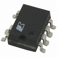
IC OFFLINE SWIT OVP UVLO 8SMD
Manufacturer
Power Integrations
Series
TOPSwitch®-FXr
Type
Off Line Switcherr
Datasheet
1.TOP234YN.pdf
(36 pages)
Specifications of TOP234GN
Output Isolation
Isolated
Frequency Range
66 ~ 132kHz
Voltage - Output
700V
Power (watts)
30W
Operating Temperature
-40°C ~ 150°C
Package / Case
8-SMD Gull Wing, 7 Leads
Output Voltage
12 V
Input / Supply Voltage (max)
265 VAC
Input / Supply Voltage (min)
85 VAC
Duty Cycle (max)
78 %
Switching Frequency
132 KHz
Supply Current
1.5 mA
Operating Temperature Range
- 40 C to + 150 C
Mounting Style
SMD/SMT
Lead Free Status / RoHS Status
Lead free / RoHS Compliant
Available stocks
Company
Part Number
Manufacturer
Quantity
Price
Company:

Part Number:
TOP234GN
Manufacturer:
PowerInt
Quantity:
350
Part Number:
TOP234GN
Manufacturer:
POWER
Quantity:
20 000
Part Number:
TOP234GN-TL
Manufacturer:
POWER
Quantity:
20 000


using a Zener clamp, 165 V when using an RCD clamp and
185 V when using RCD clamp with current limit feed forward.
For designs where operating current is significantly lower than
the default current limit, it is recommended to use an externally
set current limit close to the operating peak current to reduce
peak flux density and peak power (see Figure 17). In most
applications, the tighter current limit tolerance, higher switching
frequency and soft-start features of TOPSwitch-FX contribute
to a smaller transformer when compared to TOPSwitch-II.
Standby Consumption
Cycle skipping can significantly reduce power loss at zero load,
especially when a Zener clamp is used. For very low secondary
power consumption use a TL431 regulator for feedback control.
Alternately, switching losses can be significantly reduced by
switching from 132 kHz in normal operation to 66 kHz under
light load conditions.
TOPSwitch-FX Layout Considerations
Primary Side Connections
Use a single point (Kelvin) connection at the negative terminal
of the input filter capacitor for TOPSwitch-FX SOURCE pin
and bias winding return. This improves surge capabilities by
returning surge currents from the bias winding directly to the
input filter capacitor.
The CONTROL pin bypass capacitor should be located as close
as possible to the SOURCE and CONTROL pins and its
SOURCE connection trace should not be shared by the main
MOSFET switching currents.
All SOURCE pin referenced components connected to the
MULTI-FUNCTION pin should also be located close to
SOURCE and MULTI-FUNCTION pins with dedicated SOURCE
pin connection. The MULTI-FUNCTION pin's trace should be
kept as short as possible and away from the DRAIN trace to
prevent noise coupling. Line sense resistor (R1 in Figures 29 and
30) should be located close to the MULTI-FUNCTION pin to
minimize the trace length on the MULTI-FUNCTION pin side.
In addition to the 47 µF CONTROL pin capacitor, a high frequency
bypass capacitor in parallel may be used for better noise immunity.
The feedback optocoupler output should also be located close to
the CONTROL and SOURCE pins of TOPSwitch-FX.
Y-Capacitor
The Y-capacitor should be connected close to the secondary
output return pin(s) and the primary DC input pin of the
transformer (see Figures 29 and 30).
Heat Sinking
The tab of the Y package (TO-220) is internally electrically
tied to the SOURCE pin. To avoid circulating currents, a heat
sink attached to the tab should not be electrically tied to any
nodes on the PC board.
When using P (DIP-8) or G (SMD-8) packages, a copper area
underneath the package connected to the SOURCE pins will act
as an effective heat sink.
In addition, sufficient copper area should be provided at the
anode and cathode leads of the output diode(s) for heat sinking.
Quick Design Checklist
As with any power supply design, all TOPSwitch-FX designs
should be verified on the bench to make sure that components
specifications are not exceeded under worst case conditions.
The following minimum set of tests is strongly recommended:
1. Maximum drain voltage – Verify that peak V
2. Maximum drain current – At maximum ambient temperature,
3. Thermal check – At maximum output power, minimum
Design Tools
1. Technical literature: Data Sheet, Application Notes,
2. Transformer design spreadsheet.
3. Engineering prototype boards.
Up to date information on design tools can be found at Power
Integrations Web site: www.powerint.com
Design Ideas, etc.
exceed 675 V at highest input voltage and maximum overload
output power. Maximum overload output power occurs
when the ouput is overloaded to a level just before the power
supply goes into auto-restart (loss of regulation).
maximum input voltage and maximum output load, verify
drain current waveforms at start-up for any signs of
transformer saturation and excessive leading edge current
spikes. TOPSwitch-FX has a leading edge blanking time of
200 ns to prevent premature termination of the on-cycle.
Verify that the leading edge current spike is below the
allowed current limit envelope (see Figure 33) for the drain
current waveform at the end of the 200 ns blanking period.
input voltage and maximum ambient temperature, verify
that temperature specifications are not exceeded for
TOPSwitch-FX, transformer, output diodes and output
capacitors. Enough thermal margin should be allowed for
the part-to-part variation of the R
specified in the data sheet. The margin required can either
be calculated from the tolerances or it can be accounted for
by connecting an external resistance in series with the
DRAIN pin and attached to the same heatsink, having a
resistance value that is equal to the difference between the
measured R
maximum specification.
DS(ON)
of the device under test and the worst case
DS(ON)
TOP232-234
of TOPSwitch-FX as
DS
7/01
B
does not
23
Related parts for TOP234GN
Image
Part Number
Description
Manufacturer
Datasheet
Request
R

Part Number:
Description:
SOP-16
Manufacturer:
Power Integrations
Datasheet:
Part Number:
Description:
DIP8
Manufacturer:
Power Integrations
Datasheet:
Part Number:
Description:
TO-263
Manufacturer:
Power Integrations
Datasheet:
Part Number:
Description:
TO-263
Manufacturer:
Power Integrations
Datasheet:
Part Number:
Description:
Manufacturer:
Power Integrations
Datasheet: