AT28BV64-30JI Atmel, AT28BV64-30JI Datasheet
AT28BV64-30JI
Specifications of AT28BV64-30JI
Available stocks


Related parts for AT28BV64-30JI


AT28BV64-30JI Summary of contents
Page 1
... When the device is deselected the standby current is less than 50 µA. The AT28BV64 is accessed like a Static RAM for the read or write cycles without the need for external components. During a byte write, the address and data are latched internally, freeing the microprocessor address and data bus for other operations. Fol- lowing the initiation of a write cycle, the device will busy state and automatically clear and write the latched data using an internal control timer ...
Page 2
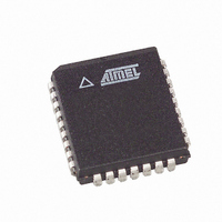
... I/O0 - I/O7 Data Inputs/Outputs RDY/BUSY Ready/Busy Output NC No Connect DC Don’t Connect 2.1 PLCC Top View I/O0 13 0493C–PEEPR–08/07 2.2 2 VCC 27 A11 RDY/BUSY A10 I/O7 21 I/O6 AT28BV64 PDIP, SOIC Top View RDY/BUSY 1 28 VCC A12 A11 A10 I/O7 I/ I/O6 I/ I/O5 I/O2 ...
Page 3
... This is a stress rating only and functional operation of the device at these or any other conditions beyond those indicated in the operational sections of this specification is not implied. Exposure to absolute maximum rating conditions for extended periods may affect + 0.6V device reliability CC AT28BV64 3 ...
Page 4
... Byte Write Writing data into the AT28BV64 is similar to writing into a Static RAM. A low pulse on the input with OE high and low (respectively) initiates a byte write. The address loca- tion is latched on the falling edge of WE (or CE); the new data is latched on the rising edge. ...
Page 5
... Input High Voltage IH V Output Low Voltage OL V Output High Voltage OH 0493C–PEEPR–08/07 AT28BV64-30 -40°C - 85°C 2. Condition MHz mA OUT for RDY/BUSY -100 µA OH AT28BV64 WE I OUT High High Z Min Max Units 5 µA 5 µA 50 µ 0.6 V 2.0 V 0.3 V 0 ...
Page 6
... ACC specified from whichever occurs first ( This parameter is characterized and is not 100% tested. AT28BV64 6 (1)(2)(3)( after the address transition without impact on t ACC after the falling edge of CE without impact pF). L AT28BV64-30 Min Max Units 300 ns 300 ns 0 150 ACC ...
Page 7
... Input Test Waveforms and Measurement Level 12. Output Test Load 13. Pin Capacitance ( MHz 25°C Symbol Typ OUT Note: 1. This parameter is characterized and is not 100% tested. 0493C–PEEPR–08/ < Max 6 12 AT28BV64 Units Conditions OUT 7 ...
Page 8
... Address Hold Time AH t Write Pulse Width ( Data Set-up Time Data, OE Hold Time DH OEH t Time to Device Busy DB t Write Cycle Time WC 15. AC Write Waveforms 15.1 WE Controlled 15.2 CE Controlled AT28BV64 8 Min Max Units 10 ns 100 ns 150 1000 ns 100 0493C–PEEPR–08/07 ...
Page 9
... Data Polling Characteristics Symbol Parameter t Data Hold Time Hold Time OEH ( Output Delay OE t Write Recovery Time WR Notes: 1. These parameters are characterized and not 100% tested. 2. See AC Characteristics. 17. Data Polling Waveforms 0493C–PEEPR–08/07 (1) Min AT28BV64 Typ Max Units ...
Page 10
... The following table lists standard Atmel Device Numbers Speed AT28BV64 30 19. Die Products Reference Section: Parallel EEPROM Die Products AT28BV64 10 Operating Voltage Ordering Code AT28BV64-30JI AT28BV64-30PI 2.7V to 3.6V AT28BV64-30SI AT28BV64-30TI Package Type ® products that can be ordered. Package and Temperature Combinations JI, PI, SI, TI Package Operation Range ...
Page 11
... Lead coplanarity is 0.004" (0.102 mm) maximum. 2325 Orchard Parkway San Jose, CA 95131 R 0493C–PEEPR–08/07 1.14(0.045) X 45˚ PIN NO. 1 IDENTIFIER TITLE 32J, 32-lead, Plastic J-leaded Chip Carrier (PLCC) AT28BV64 0.318(0.0125) 0.191(0.0075 COMMON DIMENSIONS (Unit of Measure = mm) MIN NOM MAX SYMBOL A 3.175 – ...
Page 12
... PDIP A SEATING PLANE Notes: 1. This package conforms to JEDEC reference MS-011, Variation AB. 2. Dimensions D and E1 do not include mold Flash or Protrusion. Mold Flash or Protrusion shall not exceed 0.25 mm (0.010"). 2325 Orchard Parkway San Jose, CA 95131 R AT28BV64 12 D PIN 0º ~ 15º REF eB TITLE 28P6, 28-lead (0.600" ...
Page 13
... PIN 1 1.27(0.50) BSC TOP VIEW 18.10(0.7125) 17.70(0.6969) 0.30(0.0118) 0.10(0.0040) 0º ~ 8º 1.27(0.050) 0.40(0.016) TITLE 28S, 28-lead, 0.300" Body, Plastic Gull Wing Small Outline (SOIC) JEDEC Standard MS-013 AT28BV64 10.65(0.419) 10.00(0.394) 2.65(0.1043) 2.35(0.0926) SIDE VIEWS 0.32(0.0125) 0.23(0.0091) DRAWING NO. 28S 8/4/03 REV ...
Page 14
... E Notes: 1. This package conforms to JEDEC reference MO-183. 2. Dimensions D1 and E do not include mold protrusion. Allowable protrusion 0.15 mm per side and 0.25 mm per side. 3. Lead coplanarity is 0.10 mm maximum. 2325 Orchard Parkway San Jose, CA 95131 R AT28BV64 14 PIN SEATING PLANE A1 TITLE 28T, 28-lead (8 x 13.4 mm) Plastic Thin Small Outline Package, Type I (TSOP) 0º ...
Page 15
... Disclaimer: The information in this document is provided in connection with Atmel products. No license, express or implied, by estoppel or otherwise, to any intellectual property right is granted by this document or in connection with the sale of Atmel products. EXCEPT AS SET FORTH IN ATMEL’S TERMS AND CONDI- TIONS OF SALE LOCATED ON ATMEL’S WEB SITE, ATMEL ASSUMES NO LIABILITY WHATSOEVER AND DISCLAIMS ANY EXPRESS, IMPLIED OR STATUTORY WARRANTY RELATING TO ITS PRODUCTS INCLUDING, BUT NOT LIMITED TO, THE IMPLIED WARRANTY OF MERCHANTABILITY, FITNESS FOR A PARTICULAR PURPOSE, OR NON-INFRINGEMENT ...