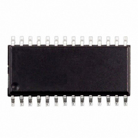
M48Z35Y-70MH1E STMicroelectronics, M48Z35Y-70MH1E Datasheet - Page 6

M48Z35Y-70MH1E
Manufacturer Part Number
M48Z35Y-70MH1E
Description
IC NVSRAM 256KBIT 70NS 28SOIC
Manufacturer
STMicroelectronics
Specifications of M48Z35Y-70MH1E
Format - Memory
RAM
Memory Type
NVSRAM (Non-Volatile SRAM)
Memory Size
256K (32K x 8)
Speed
70ns
Interface
Parallel
Voltage - Supply
4.5 V ~ 5.5 V
Operating Temperature
0°C ~ 70°C
Package / Case
28-SOIC, 28-SOH (8.48mm Width)
Data Bus Width
8 bit
Organization
32 Kb x 8
Interface Type
Parallel
Access Time
70 ns
Supply Voltage (max)
5.5 V
Supply Voltage (min)
4.5 V
Operating Current
50 mA
Maximum Operating Temperature
70 C
Minimum Operating Temperature
0 C
Mounting Style
SMD/SMT
Memory Configuration
32K X 8
Supply Voltage Range
4.5V To 5.5V
Memory Case Style
SOIC
No. Of Pins
28
Rohs Compliant
Yes
Lead Free Status / RoHS Status
Lead free / RoHS Compliant
Other names
497-2883-5
M48Z35Y-70MH1
M48Z35Y-70MH1
Available stocks
Company
Part Number
Manufacturer
Quantity
Price
M48Z35, M48Z35Y
OPERATING MODES
The M48Z35/Y also has its own Power-fail Detect
circuit. The control circuitry constantly monitors
the single 5V supply for an out of tolerance condi-
tion. When V
protects the SRAM, providing a high degree of
Table 2. Operating Modes
Note: X = V
Note: 1. See
READ Mode
The M48Z35/Y is in the READ Mode whenever W
(WRITE Enable) is high, E (Chip Enable) is low.
The device architecture allows ripple-through ac-
cess of data from eight of 264,144 locations in the
static storage array. Thus, the unique address
specified by the 15 Address Inputs defines which
one of the 32,768 bytes of data is to be accessed.
Valid data will be available at the Data I/O pins
within Address Access time (t
address input signal is stable, providing that the E
and G access times are also satisfied. If the E and
G access times are not met, valid data will be
Figure 7. READ Mode AC Waveforms
Note: WRITE Enable (W) = High.
6/20
Deselect
WRITE
READ
READ
Deselect
Deselect
Mode
IH
A0-A14
E
G
DQ0-DQ7
Table 6., page 10
or V
CC
IL
; V
is out of tolerance, the circuit write
V
SO
SO
= Battery Back-up Switchover Voltage.
4.75 to 5.5V
4.5 to 5.5V
to V
V
V
for details.
PFD
or
SO
CC
(1)
(min)
AVQV
(1)
) after the last
tAVQV
tELQX
tELQV
tGLQX
tGLQV
V
V
V
V
E
X
X
IH
IL
IL
IL
tAVAV
VALID
V
V
G
X
X
X
X
IH
data security in the midst of unpredictable system
operation brought on by low V
low approximately 3V, the control circuitry con-
nects the battery which maintains data until valid
power returns.
IL
available after the latter of the Chip Enable Access
time (t
(t
The state of the eight three-state Data I/O signals
is controlled by E and G. If the outputs are activat-
ed before t
indeterminate state until t
puts are changed while E and G remain active,
output data will remain valid for Output Data Hold
time (t
Address Access.
GLQV
AXQX
).
ELQV
V
V
V
W
X
X
X
IH
IH
IL
AVQV
) but will go indeterminate until the next
VALID
) or Output Enable Access time
, the data lines will be driven to an
DQ0-DQ7
High Z
High Z
High Z
High Z
D
D
OUT
tGHQZ
IN
AVQV
Battery Back-up Mode
CC
. If the Address In-
CMOS Standby
. As V
Standby
tAXQX
tEHQZ
Power
AI00925
Active
Active
Active
CC
falls be-


