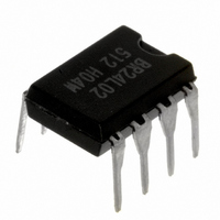
BR24L02-W Rohm Semiconductor, BR24L02-W Datasheet - Page 4

BR24L02-W
Manufacturer Part Number
BR24L02-W
Description
IC EEPROM 2KBIT 400KHZ 8DIP
Manufacturer
Rohm Semiconductor
Datasheet
1.BR24L08F-WE2.pdf
(33 pages)
Specifications of BR24L02-W
Format - Memory
EEPROMs - Serial
Memory Type
EEPROM
Memory Size
2K (256 x 8)
Speed
400kHz
Interface
I²C, 2-Wire Serial
Voltage - Supply
1.8 V ~ 5.5 V
Operating Temperature
-40°C ~ 85°C
Package / Case
8-DIP (0.300", 7.62mm)
Lead Free Status / RoHS Status
Lead free / RoHS Compliant
Available stocks
Company
Part Number
Manufacturer
Quantity
Price
Part Number:
BR24L02-W
Manufacturer:
ROHM/罗姆
Quantity:
20 000
●Sync data input / output timing
●Block diagram
●Pin assignment and description
GND
A0
A1
A2
(output)
SCL
SDA
1
2
3
4
SDA
(input)
SCL
SCL
SDA
(入力)
SDA
(出力)
○Input read at the rise edge of SCL
○Data output in sync with the fall of SCL
Fig.1-(a) Sync data input / output timing
tSU:STA
BR24L01A-W
BR24L02-W
BR24L04-W
BR24L08-W
BR24L16-W
BR24L32-W
BR24L64-W
(n-th address)
Write data
tHD:STA
tBUF
Fig.1-(c) Write cycle timing
Fig.1-(b) Start-stop bit timing
GND
*2
*2
D0
*2
A2
A1
A0
tHD:STA
ACK
2
1
3
4
tR
START BIT
8
7
5
6
*
tSU:DAT
1
Vcc
WP
SCL
SDA
Stop condition
7bit : BR24L01A-W
8bit : BR24L02-W
9bit : BR24L04-W
tPD
tF
generating circuit
tLOW
High voltage
tWR
tSU:STO
tHIGH
Terminal
7bit
8bit
9bit
10bi
Address
decoder
name
GND
SDA
SCL
WP
Vcc
A0
A1
A2
t
*1
11bit
12bit
13b
Start condition
tDH
tHD:DAT
it
10bit : BR24L08-W
11bit : BR24L16-W
12bit : BR24L32-W
13bit : BR24L64-W
Control circuit
STOP BIT
Input /
output
Input /
output
Input
Input
Input
Input
Input
*1
-
-
7bit
8bit
9bit
10bi
t
Fig.2 Block diagram
11bit
12bit
13b
START
1Kbit~64Kbit EEPROM array
it
BR24L01A-W
Reference voltage of all input / output, 0V
Slave and word address, Serial data input serial data output
Serial clock input
Write protect terminal
Connect the power source.
Slave address setting
voltage detection
Power source
Slave - word
address register
Slave address setting
○At write execution, in the area from the D0 taken clock rise of the first
○By setting WP “HIGH” in the area, write can be cancelled.
4/32
STOP
When it is set WP=“HIGH” during tWR, write is forcibly ended, and data of
address under access is not guaranteed, therefore write it once again.
DATA(1), to tWR, set WP=“LOW”.
SCL
SDA
WP
BR24L02-W
SCL
SDA
*
Slave address setting
WP
2 A0=N.C.
A0, A1=N.C.
A0, A1= N.C. A2=Don’t Use
D1
DATA(1)
D1
Fig.1-(e) WP timing at write cancel
Fig.1-(d) WP timing at write execution
tSU:WP
DATA(1)
D0
D0
ACK
BR24L04-W
ACK
ACK
register
Data
8bit
tHIGH:WP
Not connected
Function
BR24L08-W
DATA(n)
DATA(n)
: BR24L16-W
: BR24L04-W
: BR24L08-W
Not connected
ACK
BR24L16-W
Not used
ACK
ストップコンディション
8
7
6
5
Stop condition
Vcc
WP
SCL
SDA
tWR
tWR
BR24L32-W
Slave address setting
Slave address setting
Slave address setting
tHD:WP
BR24L64-W


