BR24L02-W Rohm Semiconductor, BR24L02-W Datasheet - Page 23
BR24L02-W
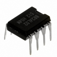
Manufacturer Part Number
BR24L02-W
Description
IC EEPROM 2KBIT 400KHZ 8DIP
Manufacturer
Rohm Semiconductor
Datasheet
1.BR24L08F-WE2.pdf
(33 pages)
Specifications of BR24L02-W
Format - Memory
EEPROMs - Serial
Memory Type
EEPROM
Memory Size
2K (256 x 8)
Speed
400kHz
Interface
I²C, 2-Wire Serial
Voltage - Supply
1.8 V ~ 5.5 V
Operating Temperature
-40°C ~ 85°C
Package / Case
8-DIP (0.300", 7.62mm)
Lead Free Status / RoHS Status
Lead free / RoHS Compliant
Available stocks
Company
Part Number
Manufacturer
Quantity
Price

Part Number:
BR24L02-W
Manufacturer:
ROHM/罗姆
Quantity:
20 000


・ As for page write cycle of BR24S32-W and BR24S64-W , after the significant 7 bits (in the case of BR24S32-W) of word address,
●Write Command
・Data is written to the address designated by word address (n-th address).
・By issuing stop bit after 8bit data input, write to memory cell inside starts.
・When internal write is started, command is not accepted for tWR (5ms at maximum).
・By page write cycle, the following can be written in bulk: Up to 16 bytes (BR24S16-W)
・As for page write command of BR24S16-W, after page select bit(PS) of slave address is designated arbitrarily, by continuing
data input of 2 bytes or more, the address of insignificant 4 bits is incremented internally, and data up to 16 bytes can be written.
or the significant 8 bits (in the case of BR24S64-W) of word address are designated arbitrarily, by continuing data input of 2 bytes
or more, the address of insignificant 5 bits is incremented internally, and data up to 32 bytes can be written.
・As for page write cycle of BR24S128-W and BR24S256-W, after the significant 9 bit (in the case of BR24S128-W) of word
address, or the significant 10bit (in the case of BR24S256-W) of word address are designated arbitrarily, by continuing data input
of 64 bytes or more.
And when data of the maximum bytes or higher is sent, data from the first byte is overwritten.
(Refer to "Internal address increment of "Notes on page write cycle" in P24/32.)
○Write cycle
・Arbitrary data is written to EEPROM. When to write only 1 byte, byte write normally used, and when to write continuous data
of 2 bytes or more, simultaneous write is possible by page write cycle. The maximum number of write bytes is specified per
device of each capacity.
Up to 64 arbitrary bytes can be written. (In the case of BR24S128/256-W)
S D A
L IN E
SDA
LINE
SDA
LINE
S D A
L IN E
S
A
R
S
A
R
S
T
A
R
T
T
T
T
T
S
T
A
R
T
Fig.36 Page write cycle (BR24S32/64/128/256-W)
1 0
1 0
1
1
Fig.34 Byte write cycle (BR24S32/64/128/256-W)
Fig.35 Page write cycle (BR24S16-W)
Fig.33 Byte write cycle (BR24S16-W)
0
A D D R E S S
0
A D D R E S S
S L A V E
1
Note)
1
N o te )
S L A V E
1
1
ADDRESS
ADDRESS
0
Note)
SLAVE
Note)
SLAVE
0
0
注 )
A 2
0
A 2
A2
A2
A 1
A 1
A 0
A1
A1
A 0
W
W
R
T
E
R
I
/
A0
A0
A
C
K
W
R
W
W
R
/
R
W
W
W
R
T
E
/
R
T
E
/
R
T
E
I
I
*
I
A
C
K
W A
1 4
A
C
K
A
C
K
A D D R E S S (n )
W A
*1
1 st W O R D
W A
13
*
7
WA
7
*1
W A
1 2
WA
14
1st WORD
ADDRESS
A D D R E S S (n )
W A
11
WA
13
W O R D
ADDRESS
WA
12
WORD
*1
WA
11
C
A
K
Note)
W A
0
WA
A D D R E S S (n )
0
2 n d W O R D
A
C
K
Fig.37 Difference of slave address each type
C
A
C
K
A
K
D 7
D7
D A T A (n )
W A
1 0
2nd WORD
0
ADDRESS
DATA
A
C
K
D 7
: Up to 32 bytes (BR24S32-W, BR24S64-W)
: Up to 64 bytes (BR24S128-W, BR24S256-W)
1
D A T A (n )
D 0
D0
0
WA
A
C
K
0
23/32
*1 *2 *3
A
C
K
A 2
A
C
K
D7
S
O
P
T
D 0
D A T A (n + 1 5 )
A 1
A
C
K
A 0
DATA
D A TA (n + 3 1 )
D 0
*2
A
C
K
*1 In BR24S16-W, A2 becomes P2
*2 In BR24S16-W, A1 becomes P1
*3 In BR24S16-W, A0 becomes P0
D0
*2
D 0
S
O
P
T
A
C
K
C
A
K
O
S
T
P
S
O
P
T
*1 As for WA12, BR24S32-W becomes Don't care.
*1 As for WA12, BR24S32-W becomes Don't care.
*2 As for BR24S128/256-W becomes (n+63).
As for WA13, BR24S32/64-W becomes Don't care.
As for WA14, BR24S32/64/128-W becomes Don't care.
As for WA13, BR24S32/64-W becomes Don't care.
As for WA14, BR24S32/64/128-W becomes Don't care.
Related parts for BR24L02-W
Image
Part Number
Description
Manufacturer
Datasheet
Request
R

Part Number:
Description:
Manufacturer:
Rohm Semiconductor
Datasheet:
Part Number:
Description:
Manufacturer:
Rohm Semiconductor
Datasheet:
Part Number:
Description:
Manufacturer:
Rohm Semiconductor
Datasheet:
Part Number:
Description:
Manufacturer:
Rohm Semiconductor
Datasheet:
Part Number:
Description:
Manufacturer:
Rohm Semiconductor
Datasheet:
Part Number:
Description:
Manufacturer:
Rohm Semiconductor
Datasheet:
Part Number:
Description:
Manufacturer:
Rohm Semiconductor
Datasheet:
Part Number:
Description:
Manufacturer:
Rohm Semiconductor
Datasheet:
Part Number:
Description:
Manufacturer:
Rohm Semiconductor
Datasheet:
Part Number:
Description:
Manufacturer:
Rohm Semiconductor
Datasheet:
Part Number:
Description:
Manufacturer:
Rohm Semiconductor
Datasheet:
Part Number:
Description:
Manufacturer:
Rohm Semiconductor
Datasheet:

Part Number:
Description:
DIODE SWITCH 80V 25MA SMD5 TR
Manufacturer:
Rohm Semiconductor
Datasheet: