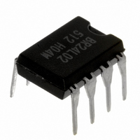
BR24L02-W Rohm Semiconductor, BR24L02-W Datasheet - Page 18

BR24L02-W
Manufacturer Part Number
BR24L02-W
Description
IC EEPROM 2KBIT 400KHZ 8DIP
Manufacturer
Rohm Semiconductor
Datasheet
1.BR24L08F-WE2.pdf
(33 pages)
Specifications of BR24L02-W
Format - Memory
EEPROMs - Serial
Memory Type
EEPROM
Memory Size
2K (256 x 8)
Speed
400kHz
Interface
I²C, 2-Wire Serial
Voltage - Supply
1.8 V ~ 5.5 V
Operating Temperature
-40°C ~ 85°C
Package / Case
8-DIP (0.300", 7.62mm)
Lead Free Status / RoHS Status
Lead free / RoHS Compliant
Available stocks
Company
Part Number
Manufacturer
Quantity
Price
Part Number:
BR24L02-W
Manufacturer:
ROHM/罗姆
Quantity:
20 000
* When using at Ta=25℃ or higher, 4.5mW(*1,*2) 3.0mW(*3,*7) 3.3mW(*4) 3.1mW(*5,*6) to be
reduced per 1℃
●Absolute maximum ratings (Ta=25℃)
●Electrical characteristics
(Unless otherwise specified, Ta=
○Radiation resistance design is not made.
●Sync data input/output timing
SCL
SDA
SCL
SDA
"H" Input Voltage1
"L" Input Voltage1
"L" Output Voltage1
"L" Output Voltage2
Input Leakage Current
Output Leakage Current
Current consumption
at action
Standby Current
Impressed voltage
temperature range
temperature range
WRITE DATA(n)
(Output)
(Input)
Terminal Voltage
SCL
SDA
(出力)
tSU:STA
SDA
(入力)
Parameter
Permissible
○Input read at the rise edge of SCL
○Data output in sync with the fall of SCL
dissipation
Parameter
Storage
Action
tHD:STA
D0
Fig.1-(a) Sync data input / output timing
tBUF
Fig.1-(c) Write cycle timing
Fig.1-(b) Start - stop bit timing
tHD:STA
ACK
Symbol
V
V
V
V
I
I
I
I
CC1
CC2
I
LO
SB
OL1
OL2
START BIT
IH1
IL1
LI
CONDITION
tR
STOP
0.7Vcc
tSU:DAT
-0.3
Min
-1
-1
-
-
-
-
-
-
Symbol
Topr
Tstg
Vcc
Limits
Pd
Typ.
-
tPD
tF
t
-
-
-
-
-
-
-
-
-
-
tSU:STO
WR
tLOW
-
CONDITION
40~+85℃, Vcc=1.7~5.5V)
Vcc+1.0
tHIGH
0.3Vcc
START
Max.
0.4
0.2
2.0
2.5
0.5
2.0
1
1
- 0.3 ~ +6.5
450(SOP8)
450(SOP-J8)
300(SSOP-B8)
330(TSSOP-B8)
310(MSOP8)
310(TSSOP-B8J)
300(VSON008X2030)
- 65 ~ +125
- 40 ~ +85
- 0.3 ~ Vcc + 1.0
tDH
Unit
mA
mA
µA
µA
µA
V
V
V
V
tHD:DAT
STOP BIT
I
I
V
V
Vcc=5.5V , f
Byte Write, Page Write
BR24S16/32/64-W
Vcc=5.5V , f
Byte Write, Page Write
BR24S128/256-W
Vcc=5.5V , f
Random read, Current read, Sequential read
Vcc=5.5V , SDA・SCL=Vcc
A0, A1, A2=GND, WP=GND
OL
OL
IN
OUT
=3.0mA , 2.5V≦Vcc≦5.5V (SDA)
=0.7mA , 1.7V≦Vcc≦2.5V (SDA)
=0~Vcc
=0~Vcc (SDA)
Limits
SCL
SCL
SCL
=400kHz, tWR=5ms
=400kHz, tWR=5ms
=400kHz
Condition
*3
*2
*6
*1
*4
*5
*7
Unit
mW
℃
℃
V
V
SCL
SDA
WP
18/32
○At write execution, in the area from the D0 taken clock rise of the first DATA(1), to tWR, set
WP= 'LOW'.
○By setting WP "HIGH" in the area, write can be cancelled.
When it is set WP = 'HIGH' during tWR, write is forcibly ended, and data of address under access
is not guaranteed, therefore write it once again.
SCL
SDA
WP
*1 : Not 100% TESTED
D1
●Memory cell characteristics (Ta=25℃
●Recommended operating condition
●Action timing characteristics
(Unless otherwise specified, Ta=
DATA(1)
*1 : Not 100% TESTED
SCL Frequency
Data clock "High" time
Data clock "Low" time
SDA, SCL rise time
SDA, SCL fall time
Start condition hold time
Start condition setup time
Input data hold time
Input data setup time
Output data delay time
Output data hold time
Stop condition data setup time
Bus release time before transfer start
Internal write cycle time
Noise removal valid period (SDA,SCL terminal)
WP hold time
WP setup time
WP valid time
tSU:WP
D1
Number of data rewrite
Power source voltage
Data hold years
DATA(1)
D0
D0
Input voltage
Fig.1-(e) WP timing at write cancel
Parameter
times
ACK
Parameter
Fig.1-(d) WP timing at write execution
Parameter
ACK
*1
*1
*1
tHIGH:WP
DATA(n)
DATA(n)
*1
1,000,000
ACK
Stop condition
ストップコンディション
Symbol
tHIGH:WP
Min.
Symbol
tHD:STA
tSU:STA
tHD:DAT
tSU:DAT
tSU:STO
tHD:WP
ACK
-
tSU:WP
40
tHIGH
Vcc
tLOW
fSCL
tBUF
V
tWR
40~+85℃, Vcc=1.7~5.5V)
tPD
tDH
tR
tF
tI
IN
tWR
Limits
tWR
Min.
tWR
100
,
0.6
1.2
0.6
0.6
0.1
0.1
0.6
1.2
0.1
1.0
-
-
-
-
-
Typ.
0
0
Vcc=1.7V~5.5V)
-
-
tHD:WP
1.7~5.5
0~Vcc
Limits
Limits
Typ.
-
-
-
-
-
-
-
-
-
-
-
-
-
-
-
-
-
-
Max.
-
-
Max.
400
0.3
0.3
0.9
0.1
-
-
-
-
-
-
-
-
-
-
-
-
5
Times
Years
Unit
Unit
Unit
V
kHz
ms
µs
µs
µs
µs
µs
µs
ns
ns
µs
µs
µs
µs
µs
ns
µs
µs


