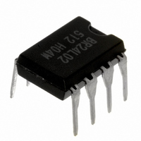
BR24L02-W Rohm Semiconductor, BR24L02-W Datasheet - Page 13

BR24L02-W
Manufacturer Part Number
BR24L02-W
Description
IC EEPROM 2KBIT 400KHZ 8DIP
Manufacturer
Rohm Semiconductor
Datasheet
1.BR24L08F-WE2.pdf
(33 pages)
Specifications of BR24L02-W
Format - Memory
EEPROMs - Serial
Memory Type
EEPROM
Memory Size
2K (256 x 8)
Speed
400kHz
Interface
I²C, 2-Wire Serial
Voltage - Supply
1.8 V ~ 5.5 V
Operating Temperature
-40°C ~ 85°C
Package / Case
8-DIP (0.300", 7.62mm)
Lead Free Status / RoHS Status
Lead free / RoHS Compliant
Available stocks
Company
Part Number
Manufacturer
Quantity
Price
Part Number:
BR24L02-W
Manufacturer:
ROHM/罗姆
Quantity:
20 000
●I/O peripheral circuit
●A0, A1, A2, WP process
○Minimum value of R
○Pull up resistance of SCL terminal
○Process of device address terminals (A0,A1,A2)
○Process of WP terminal
○Pull up resistance of SDA terminal
○Maximum value of R
SDA is NMOS open drain, so requires pull up resistance. As for this resistance value (R
value from microcontroller V
larger the consumption current at action.
When SCL control is made at CMOS output port, there is no need, but in the case there is timing where SCL becomes 'Hi-Z', add a pull up
resistance. As for the pull up resistance, one of several kΩ ~ several ten kΩ is recommended in consideration of drive performance of
output port of microcontroller.
Check whether the set device address coincides with device address input sent from the master side or not, and select one among plural
devices connected to a same bus. Connect this terminal to pull up or pull down, or Vcc or GND. And, pins (N, C, PIN) not used as device
address may be set to any of 'H' , 'L', and 'Hi-Z'.
WP terminal is the terminal that prohibits and permits write in hardware manner. In 'H' status, only READ is available and WRITE of all
address is prohibited. In the case of 'L', both are available. In the case of use it as an ROM, it is recommended to connect it to pull up or Vcc.
In the case to use both READ and WRITE, control WP terminal or connect it to pull down or GND.
The maximum value of R
The minimum value of R
(1)SDA rise time to be determined by the capacitance (CBUS) of bus line of R
(2)The bus electric potential A to be determined by input leak total (I
(2)V
(1)When IC outputs LOW, it should be satisfied that V
And AC timing should be satisfied even when SDA rise time is late.
should sufficiently secure the input 'H' level (V
OLMAX
Types with N.C.PIN
V
Ex. ) When V
OLMAX
Vcc - I
Ex. ) When V
=0.4V should secure the input 'L' level (V
from (1)
≦ V
from (2)
L
R
And
PU
V
PU
CC
∴ R
IL
PU
R
- 0.2Vcc ≧ V
CC
-0.1 V
-V
PU
CC
=3V, V
PU
R
PU
R
=3V, I
OL
PU
PU
V
is determined by the following factors.
PU
V
is determined by the following factors.
IL
IL
OL
, I
CC
≦ 300 [kΩ]
=
≦
≧
≧ 867 [Ω]
OL
L
≦ I
= 0.4 [V]
= 0.3×3
= 0.9 [V]
, and V
L
=0.4V, I
=10μA, V
BR24L16/F/FJ/FV/FVT/FVM/FVJ-W
BR24L08/F/FJ/FV/FVT/FVM/FVJ/NUX-W
BR24L04/F/FJ/FV/FVT/FVM/FVJ/NUX-W
0.8Vcc-V
OL
0.8×3-0.7×3
IH
3-0.4
3×10
OL
10×10
OL
I
-I
L
=3mA, microcontroller, EEPROM V
OL
IH
characteristics of this IC. If R
=0.7 V
-3
IH
-6
IH
Therefore, the condition (2) is satisfied.
) of microcontroller and EEPROM including recommended noise margin 0.2Vcc.
CC
IL
) of microcontroller and EEPROM including recommended noise margin 0.1Vcc.
∴ R
,
OLMAX
PU
=0.4V and I
≦
13/32
V
C
-V
I
OL
OL
OLMAX
L
) of device connected to bus at output of 'H' to SDA bus and R
PU
Microcontroller
is large, action frequency is limited. The smaller the R
IL
=3mA.
=0.3Vcc
PU
A0, A1
A0
A0, A1, A2
and SDA should be tR or below.
マイコン
PU
), select an appropriate value to this resistance
IL
Fig.52 I/O circuit diagram
バスライン容量
R
PU
Bus line
capacity
CBUS
CBUS
A
IL
BR24LXX
SDA terminal
PU
, the
PU


