74LVC595ABQ,115 NXP Semiconductors, 74LVC595ABQ,115 Datasheet - Page 12
74LVC595ABQ,115
Manufacturer Part Number
74LVC595ABQ,115
Description
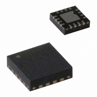
IC 8BIT SHIFT REGISTER 16HVQFN
Manufacturer
NXP Semiconductors
Series
74LVCr
Type
Not Requiredr
Datasheet
1.74LVC595ABQ115.pdf
(19 pages)
Specifications of 74LVC595ABQ,115
Package / Case
16-VQFN Exposed Pad, 16-HVQFN, 16-SQFN, 16-DHVQFN
Logic Type
Shift Register
Output Type
Standard
Function
Serial to Parallel
Number Of Elements
1
Number Of Bits Per Element
8
Voltage - Supply
1.65 V ~ 3.6 V
Operating Temperature
-40°C ~ 125°C
Mounting Type
Surface Mount
Counting Sequence
Serial to Serial/Parallel
Number Of Circuits
1
Logic Family
LVC
Propagation Delay Time
4.7 ns, 4 ns
Supply Voltage (max)
3.6 V
Maximum Operating Temperature
+ 125 C
Minimum Operating Temperature
- 40 C
Mounting Style
SMD/SMT
Operating Supply Voltage
1.8 V, 2.5 V, 3.3 V
Technology
CMOS
Number Of Elements
1
Number Of Bits
8
Logical Function
Shift Register
Operating Supply Voltage (typ)
1.8/2.5/3.3V
Operating Temp Range
-40C to 125C
Operating Supply Voltage (max)
3.6V
Operating Temperature Classification
Automotive
Mounting
Surface Mount
Pin Count
16
Lead Free Status / RoHS Status
Lead free / RoHS Compliant
Lead Free Status / RoHS Status
Lead free / RoHS Compliant, Lead free / RoHS Compliant
Other names
74LVC595ABQ-G
74LVC595ABQ-G
935282468115
74LVC595ABQ-G
935282468115


NXP Semiconductors
Table 8.
74LVC595A_1
Product data sheet
Supply voltage
V
V
V
Fig 11. The master reset (MR) pulse width, the master reset to serial data output (Q7S) propagation delays and the
Fig 12. 3-state enable and disable times
CC
CC
CC
< 2.7 V
2.7 V
Measurement points are given in
V
master reset to shift clock (SHCP) recovery time
Measurement points are given in
V
OL
OL
Measurement points
and V
and V
OH
OH
are typical output voltage drops that occur with the output load.
are typical output voltage drops that occur with the output load.
HIGH-to-OFF
OFF-to-HIGH
OFF-to-LOW
LOW-to-OFF
OE input
output
output
Input
V
0.5
1.5 V
M
SH CP input
Q 7 S output
MR input
V
CC
Table
Table
GND
GND
V
V
V
CC
OH
OL
V
GND
GND
V
I
V
OH
OL
8.
8.
V
V
I
I
V
Rev. 01 — 29 May 2007
M
enabled
outputs
V
t
8-bit serial-in/serial-out or parallel-out shift register; 3-state
PLZ
Output
V
0.5
1.5 V
t
M
PHZ
M
t
t
PHL
W
V
CC
V
X
V
V
t
M
Y
rec
V
M
disabled
outputs
V
V
V
t
X
OL
OL
PZL
t
PZH
0.15 V
0.3 V
mna561
V
M
V
M
001aae821
outputs
enabled
74LVC595A
V
V
V
Y
OH
OH
© NXP B.V. 2007. All rights reserved.
0.15 V
0.3 V
12 of 19
Related parts for 74LVC595ABQ,115
Image
Part Number
Description
Manufacturer
Datasheet
Request
R

Part Number:
Description:
74lvc595a 8-bit Serial-in/serial-out Or Parallel-out Shift Register; 3-state
Manufacturer:
NXP Semiconductors
Datasheet:
Part Number:
Description:
NXP Semiconductors designed the LPC2420/2460 microcontroller around a 16-bit/32-bitARM7TDMI-S CPU core with real-time debug interfaces that include both JTAG andembedded trace
Manufacturer:
NXP Semiconductors
Datasheet:

Part Number:
Description:
NXP Semiconductors designed the LPC2458 microcontroller around a 16-bit/32-bitARM7TDMI-S CPU core with real-time debug interfaces that include both JTAG andembedded trace
Manufacturer:
NXP Semiconductors
Datasheet:
Part Number:
Description:
NXP Semiconductors designed the LPC2468 microcontroller around a 16-bit/32-bitARM7TDMI-S CPU core with real-time debug interfaces that include both JTAG andembedded trace
Manufacturer:
NXP Semiconductors
Datasheet:
Part Number:
Description:
NXP Semiconductors designed the LPC2470 microcontroller, powered by theARM7TDMI-S core, to be a highly integrated microcontroller for a wide range ofapplications that require advanced communications and high quality graphic displays
Manufacturer:
NXP Semiconductors
Datasheet:
Part Number:
Description:
NXP Semiconductors designed the LPC2478 microcontroller, powered by theARM7TDMI-S core, to be a highly integrated microcontroller for a wide range ofapplications that require advanced communications and high quality graphic displays
Manufacturer:
NXP Semiconductors
Datasheet:
Part Number:
Description:
The Philips Semiconductors XA (eXtended Architecture) family of 16-bit single-chip microcontrollers is powerful enough to easily handle the requirements of high performance embedded applications, yet inexpensive enough to compete in the market for hi
Manufacturer:
NXP Semiconductors
Datasheet:
Part Number:
Description:
The XA-S3 device is a member of Philips Semiconductors? XA(eXtended Architecture) family of high performance 16-bitsingle-chip microcontrollers
Manufacturer:
NXP Semiconductors
Datasheet:

Part Number:
Description:
The NXP BlueStreak LH75401/LH75411 family consists of two low-cost 16/32-bit System-on-Chip (SoC) devices
Manufacturer:
NXP Semiconductors
Datasheet:
Part Number:
Description:
The NXP LPC3130/3131 combine an 180 MHz ARM926EJ-S CPU core, high-speed USB2
Manufacturer:
NXP Semiconductors
Datasheet:
Part Number:
Description:
The NXP LPC3141 combine a 270 MHz ARM926EJ-S CPU core, High-speed USB 2
Manufacturer:
NXP Semiconductors
Part Number:
Description:
The NXP LPC3143 combine a 270 MHz ARM926EJ-S CPU core, High-speed USB 2
Manufacturer:
NXP Semiconductors

Part Number:
Description:
The NXP LPC3152 combines an 180 MHz ARM926EJ-S CPU core, High-speed USB 2
Manufacturer:
NXP Semiconductors
Part Number:
Description:
The NXP LPC3154 combines an 180 MHz ARM926EJ-S CPU core, High-speed USB 2
Manufacturer:
NXP Semiconductors